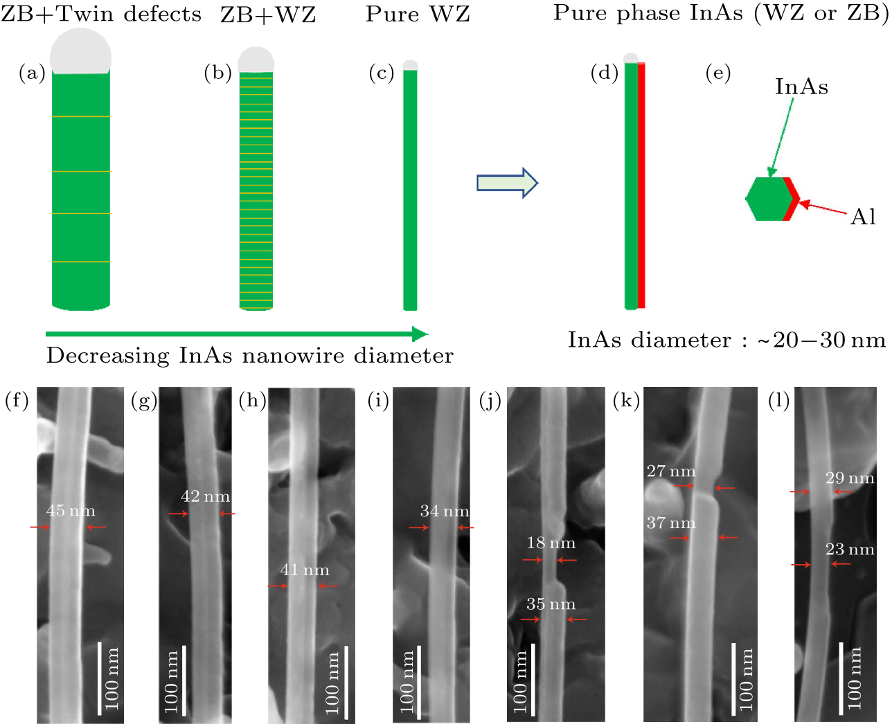
Fig. 1. In situ epitaxy of Al half shells on the ultra-thin InAs nanowires. (a)–(c) Schematic illustration of the diameter dependent InAs nanowire crystal structures. As the InAs diameter becomes thinner, the crystal structure can be tuned from a ZB crystal phase with twin defects to a mixture of the WZ and ZB phases, and finally to a pure WZ crystal phase with no stacking faults or twin defects. The yellow lines in (a) and (b) denote the twin defects and stacking faults. (d) Schematic illustration of in situ epitaxy of Al half shells on an ultra-thin InAs nanowire. The nanowire is pure phase and can be either WZ or ZB for various growth directions. (e) Schematic cross-section of InAs-Al. (f)–(j) SEM images of several typical ultra-thin InAs-Al nanowires with various wire diameters. The Al shell thickness is $\sim $17 nm. The missing of Al on part of the InAs nanowire in (j) was due to the shadow effect of another wire in front of it during the Al growth. (k)–(l) Two more shadow InAs-Al wires (from different growths) with the Al shell thickness being $\sim $10 nm and 6 nm, respectively. All the SEM images were taken at a tilt angle of 25$^{\circ}$.
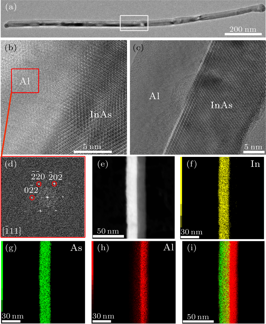
Fig. 2. Crystal structure and chemical composition of the ultra-thin InAs-Al nanowires. (a) Low-magnification TEM image of an InAs-Al nanowire. (b) and (c) High-resolution TEM images of the InAs-Al nanowire. (d) The FFT of the Al segment viewed along the $[\bar{1}11]$ axis. (e) HAADF-STEM image taken from the middle section of the InAs-Al nanowire. The white rectangle in (a) highlights the region where HAADF-STEM image was recorded. (f)–(h) False-color EDS elemental maps of In (yellow), As (green), and Al (red) taken in the middle region of the InAs-Al nanowire, respectively. (i) False-color overlay EDS elemental maps of In (yellow), As (green), and Al (red).
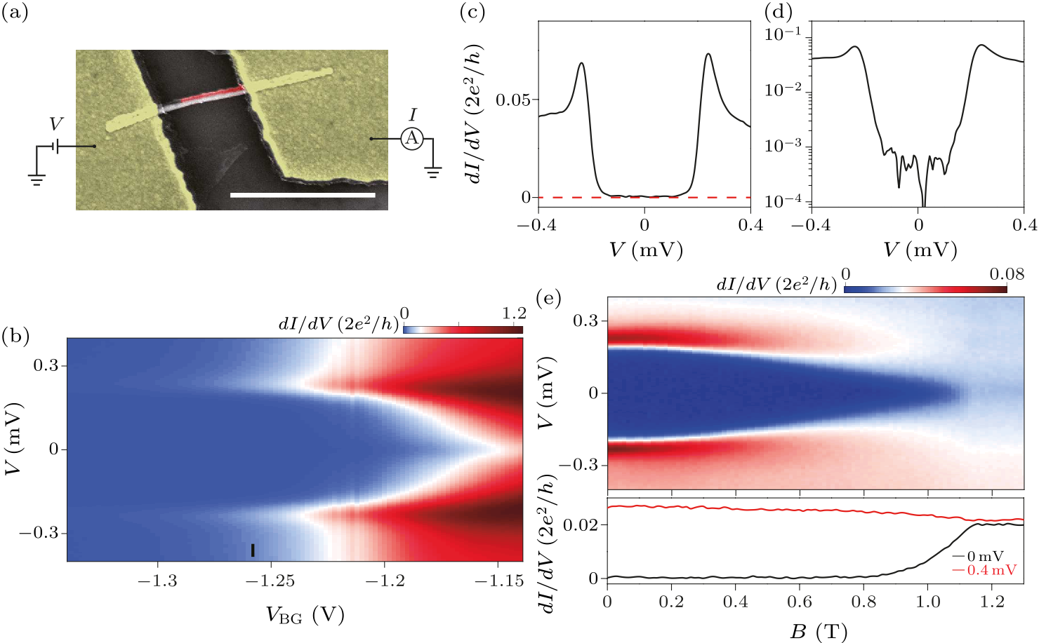
Fig. 3. Hard superconducting gap. (a) False-color SEM image of an N-NW-S device (device A). Scale bar is 1 µm. Part of the Al film (red) on the ultra-thin InAs nanowire (grey) was selectively etched. The nanowire was then contacted by normal metal (yellow, 10 nm Ti and 70 nm Au). The substrate is p-doped Si, acting as a global back gate, covered by 285-nm-thick SiO$_{2}$ (gate dielectric). Fridge base temperature is $\sim $20 mK for all the measurements with various fridge filters. (b) Differential conductance $dI/dV$ of device A as a function of bias voltage $V$ and back gate voltage $V_{\rm BG}$ resolving the superconducting gap of $\varDelta \sim 0.24$ meV. (c) and (d) Vertical line-cuts (linear and log-scale) at $V_{\rm BG}$ of $-1.258$ V labeled by the black bar in panel (b), resolving a hard superconducting gap. (e) $B$ dependence of the gap with $B$ direction aligned with the wire axis. Lower panel shows the horizontal line-cuts within the gap (0 bias, black curve) and outside the gap ($V = 0.4$ mV, red curve).
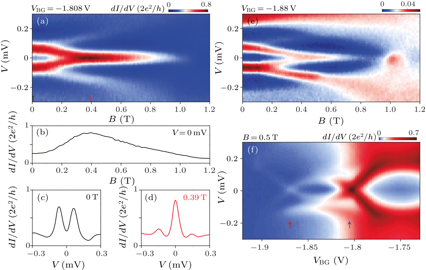
Fig. 4. Large zero bias peak. (a) Behavior of $dI/dV$ of device A shows a large zero bias peak (ZBP) at a $V_{\rm BG}$ of $-1.808$ V. (b) Zero-bias line-cut shows the peak height exceeding 80% of 2$e^{2}/h$. (c) and (d) The $dI/dV$ curve (vertical line-cut) at 0 T and 0.39 T, respectively. (e) Another ZBP remains non-split against the $B$-sweep at a different $V_{\rm BG}$ of $-1.88$ V. (f) $V_{\rm BG}$ sweep of the two ZBPs from (a) and (e) at $B = 0.5$ T. The blue and red arrows roughly correspond to the gate voltages of (a) and (e), respectively, with a small gate sweep hysteresis.
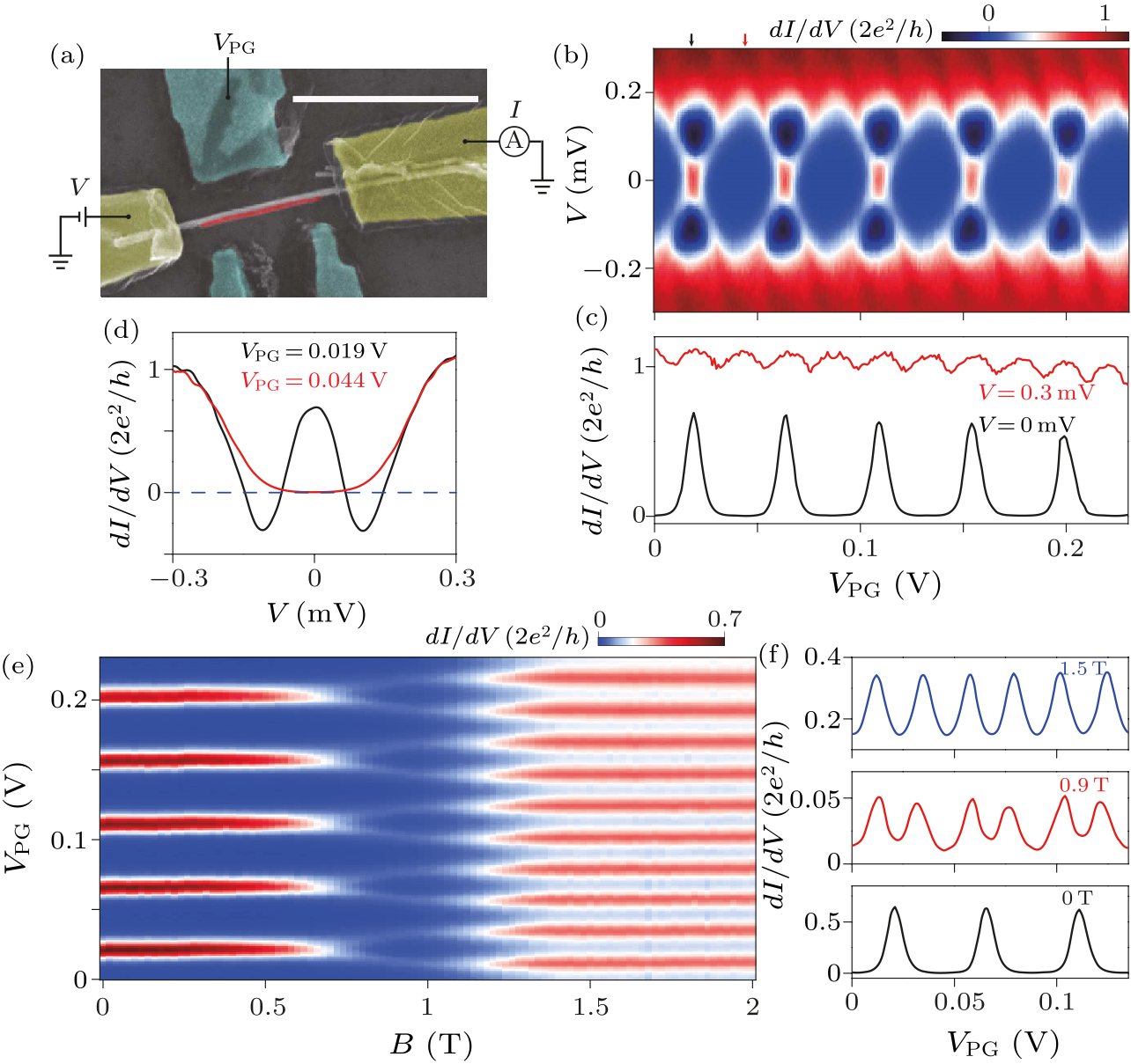
Fig. 5. The 2$e$-periodic Coulomb blockade and $2e$–$1e$ transition of an island device. (a) False-color SEM image of an InAs-Al island device (device B). Scale bar is 1 µm. The Al island (red) was defined by wet chemical etching. The normal metal contact (yellow) and side gates (cyan) are Ti/Au (10 nm/70 nm). The plunger gate voltage $V_{\rm PG}$ tunes electron number on the island, while the lower two tunnel gates tune the tunnel coupling between the island and the contacts. (b) Characteristics of $dI/dV$ of device B as a function of $V$ and $V_{\rm PG}$, revealing regular Coulomb-blockade diamonds. The two tunnel gates and back gate were kept grounded for the measurement. (c) Horizontal line-cuts at $V = 0$ mV (black curve) and $V = 0.3$ mV (red curve). (d) Vertical line-cuts at the Coulomb valley (red curve) and Coulomb peak degeneracy point (black curve) indicated by the corresponding arrow in (b). (e) Behavior of $dI/dV$ (at $V = 0$) as a function of $V_{\rm PG}$ and $B$ (direction along the nanowire), revealing the $2e$–$1e$ transition, with the vertical line-cuts at different $B$ values shown in (f).
| [1] | Lutchyn R M, Sau J D, and Das S S 2010 Phys. Rev. Lett. 105 077001 | Majorana Fermions and a Topological Phase Transition in Semiconductor-Superconductor Heterostructures
| [2] | Oreg Y, Refael G, and von Oppen F 2010 Phys. Rev. Lett. 105 177002 | Helical Liquids and Majorana Bound States in Quantum Wires
| [3] | Freedman M H, Kitaev A, Larsen M J, and Wang Z H 2003 Bull. Amer. Math. Soc. 40 31 | Topological quantum computation
| [4] | Read N and Green D 2000 Phys. Rev. B 61 10267 | Paired states of fermions in two dimensions with breaking of parity and time-reversal symmetries and the fractional quantum Hall effect
| [5] | Kitaev A Y 2001 Phys.-Usp. 44 131 | Unpaired Majorana fermions in quantum wires
| [6] | Fu L and Kane C L 2008 Phys. Rev. Lett. 100 096407 | Superconducting Proximity Effect and Majorana Fermions at the Surface of a Topological Insulator
| [7] | Lutchyn R M, Bakkers E P, Kouwenhoven L P, Krogstrup P, Marcus C M, and Oreg Y 2018 Nat. Rev. Mater. 3 52 | Majorana zero modes in superconductor–semiconductor heterostructures
| [8] | Zhang H, Liu D E, Wimmer M, and Kouwenhoven L P 2019 Nat. Commun. 10 5128 | Next steps of quantum transport in Majorana nanowire devices
| [9] | Prada E, San-Jose P, de Moor M W, Geresdi A, Lee E J, Klinovaja J, Loss D, Nygård J, Aguado R, and Kouwenhoven L P 2020 Nat. Rev. Phys. 2 575 | From Andreev to Majorana bound states in hybrid superconductor–semiconductor nanowires
| [10] | Mourik V, Zuo K, Frolov S M, Plissard S R, Bakkers E P A M, and Kouwenhoven L P 2012 Science 336 1003 | Signatures of Majorana Fermions in Hybrid Superconductor-Semiconductor Nanowire Devices
| [11] | Deng M T, Yu C L, Huang G Y, Larsson M, Caroff P, and Xu H Q 2012 Nano Lett. 12 6414 | Anomalous Zero-Bias Conductance Peak in a Nb–InSb Nanowire–Nb Hybrid Device
| [12] | Das A, Ronen Y, Most Y, Oreg Y, Heiblum M, and Shtrikman H 2012 Nat. Phys. 8 887 | Zero-bias peaks and splitting in an Al–InAs nanowire topological superconductor as a signature of Majorana fermions
| [13] | Rokhinson L P, Liu X, and Furdyna J K 2012 Nat. Phys. 8 795 | The fractional a.c. Josephson effect in a semiconductor–superconductor nanowire as a signature of Majorana particles
| [14] | Churchill H O H, Fatemi V, Grove-Rasmussen K, Deng M T, Caroff P, Xu H Q, and Marcus C M 2013 Phys. Rev. B 87 241401 | Superconductor-nanowire devices from tunneling to the multichannel regime: Zero-bias oscillations and magnetoconductance crossover
| [15] | Chang W, Albrecht S M, Jespersen T S, Kuemmeth F, Krogstrup P, Nygård J, and Marcus C M 2015 Nat. Nanotechnol. 10 232 | Hard gap in epitaxial semiconductor–superconductor nanowires
| [16] | Heedt S, Quintero-Pérez M, Borsoi F, Fursina A, van Loo N, Mazur G P, Nowak M P, Ammerlaan M, Li K, Korneychuk S, Shen J, van de An Y P M, Badawy G, Gazibegovic S, de Jong N, Aseev P, van Hoogdalem K, Bakkers E P A M, and Kouwenhoven L P 2021 Nat. Commun. 12 4914 | Shadow-wall lithography of ballistic superconductor–semiconductor quantum devices
| [17] | Pendharkar M, Zhang B, Wu H, Zarassi A, Zhang P, Dempsey C P, Lee J S, Harrington S D, Badawy G, Gazibegovic S, Op H V R L M, Rossi M, Jung J, Chen A H, Verheijen M A, Hocevar M, Bakkers E P A M, Palmstrøm C J, and Frolov S M 2021 Science 372 508 | Parity-preserving and magnetic field–resilient superconductivity in InSb nanowires with Sn shells
| [18] | Kanne T, Marnauza M, Olsteins D, Carrad D J, Sestoft J E, de Bruijckere J, Zeng L, Johnson E, Olsson E, Grove-Rasmussen K, and Nygård J 2021 Nat. Nanotechnol. 16 776 | Epitaxial Pb on InAs nanowires for quantum devices
| [19] | Stanescu T D and Das S S 2013 Phys. Rev. B 87 180504(R) | Superconducting proximity effect in semiconductor nanowires
| [20] | Takei S, Fregoso B M, Hui H, Lobos A M, and Das S S 2013 Phys. Rev. Lett. 110 186803 | Soft Superconducting Gap in Semiconductor Majorana Nanowires
| [21] | Krogstrup P, Ziino N L B, Chang W, Albrecht S M, Madsen M H, Johnson E, Nygård J, Marcus C M, and Jespersen T S 2015 Nat. Mater. 14 400 | Epitaxy of semiconductor–superconductor nanowires
| [22] | Kang J H, Grivnin A, Bor E, Reiner J, Avraham N, Ronen Y, Cohen Y, Kacman P, Shtrikman H, and Beidenkopf H 2017 Nano Lett. 17 7520 | Robust Epitaxial Al Coating of Reclined InAs Nanowires
| [23] | Carrad D J, Bjergfelt M, Kanne T, Aagesen M, Krizek F, Fiordaliso E M, Johnson E, Nygård J, and Jespersen T S 2020 Adv. Mater. 32 1908411 | Shadow Epitaxy for In Situ Growth of Generic Semiconductor/Superconductor Hybrids
| [24] | Vaitiekėnas S, Liu Y, Krogstrup P, and Marcus C M 2021 Nat. Phys. 17 43 | Zero-bias peaks at zero magnetic field in ferromagnetic hybrid nanowires
| [25] | Sestoft J E, Kanne T, Gejl A N, von Soosten M, Yodh J S, Sherman D, Tarasinski B, Wimmer M, Johnson E, Deng M T, Nygå R J, Jespersen T S, Marcus C M, and Krogstrup P 2018 Phys. Rev. Mater. 2 044202 | Engineering hybrid epitaxial InAsSb/Al nanowires for stronger topological protection
| [26] | Khan S A, Lampadaris C, Cui A, Stampfer L, Liu Y, Pauka S J, Cachaza M E, Fiordaliso E M, Kang J H, Korneychuk S, Mutas T, Sestoft J E, Krizek F, Tanta R, Cassidy M C, Jespersen T S, and Krogstrup P 2020 ACS Nano 14 14605 | Highly Transparent Gatable Superconducting Shadow Junctions
| [27] | Vaitiekėnas S, Whiticar A M, Deng M T, Krizek F, Sestoft J E, Palmstrøm C J, Martí-Sánchez S, Arbiol J, Krogstrup P, Casparis L, and Marcus C M 2018 Phys. Rev. Lett. 121 147701 | Selective-Area-Grown Semiconductor-Superconductor Hybrids: A Basis for Topological Networks
| [28] | Lee J S, Choi S, Pendharkar M, Pennachio D J, Markman B, Seas M, Koelling S, Verheijen M A, Casparis L, Petersson K D, Petkovic I, Schaller V, Rodwell M J W, Marcus C M, Krogstrup P, Kouwenhoven L P, Bakkers E P A M, and Palmstrøm C J 2019 Phys. Rev. Mater. 3 084606 | Selective-area chemical beam epitaxy of in-plane InAs one-dimensional channels grown on InP(001), InP(111)B, and InP(011) surfaces
| [29] | Stiles M D and Hamann D R 1990 Phys. Rev. B 41 5280 | Electron transmission through silicon stacking faults
| [30] | Stiles M D and Hamann D R 1988 Phys. Rev. B 38 2021 | Ballistic electron transmission through interfaces
| [31] | Nilsson M, Namazi L, Lehmann S, Leijnse M, Dick K A, and Thelander C 2016 Phys. Rev. B 93 195422 | Single-electron transport in InAs nanowire quantum dots formed by crystal phase engineering
| [32] | Prada E, San-Jose P, and Aguado R 2012 Phys. Rev. B 86 180503 | Transport spectroscopy of nanowire junctions with Majorana fermions
| [33] | Kells G, Meidan D, and Brouwer P W 2012 Phys. Rev. B 86 100503 | Near-zero-energy end states in topologically trivial spin-orbit coupled superconducting nanowires with a smooth confinement
| [34] | Liu C X, Sau J D, Stanescu T D, and Das S S 2017 Phys. Rev. B 96 075161 | Andreev bound states versus Majorana bound states in quantum dot-nanowire-superconductor hybrid structures: Trivial versus topological zero-bias conductance peaks
| [35] | Akiyama T, Sano K, Nakamura K, and Ito T 2006 Jpn. J. Appl. Phys. 45 L275 | An Empirical Potential Approach to Wurtzite-Zinc-Blende Polytypism in Group III-V Semiconductor Nanowires
| [36] | Caroff P, Dick K A, Johansson J, Messing M E, Deppert K, and Samuelson L 2009 Nat. Nanotechnol. 4 50 | Controlled polytypic and twin-plane superlattices in iii–v nanowires
| [37] | Shtrikman H, Popovitz-Biro R, Kretinin A, Houben L, Heiblum M, Bukała M, Galicka M, Buczko R, and Kacman P 2009 Nano Lett. 9 1506 | Method for Suppression of Stacking Faults in Wurtzite III−V Nanowires
| [38] | Pan D, Fu M Q, Yu X Z, Wang X L, Zhu L J, Nie S H, Wang S L, Chen Q, Xiong P, von Molnár S, and Zhao J H 2014 Nano Lett. 14 1214 | Controlled Synthesis of Phase-Pure InAs Nanowires on Si(111) by Diminishing the Diameter to 10 nm
| [39] | Güsken N A, Rieger T, Zellekens P, Bennemann B, Neumann E, Lepsa M I, Schäpers T, and Grützmacher D 2017 Nanoscale 9 16735 | MBE growth of Al/InAs and Nb/InAs superconducting hybrid nanowire structures
| [40] | Moore C, Stanescu T D, and Tewari S 2018 Phys. Rev. B 97 165302 | Two-terminal charge tunneling: Disentangling Majorana zero modes from partially separated Andreev bound states in semiconductor-superconductor heterostructures
| [41] | Vuik A, Nijholt B, Akhmerov A, and Wimmer M 2019 SciPost Phys. 7 61 | Reproducing topological properties with quasi-Majorana states
| [42] | Antipov A E, Bargerbos A, Winkler G W, Bauer B, Rossi E, and Lutchyn R M 2018 Phys. Rev. X 8 031041 | Effects of Gate-Induced Electric Fields on Semiconductor Majorana Nanowires
| [43] | Mikkelsen A E G, Kotetes P, Krogstrup P, and Flensberg K 2018 Phys. Rev. X 8 031040 | Hybridization at Superconductor-Semiconductor Interfaces
| [44] | Woods B D, Stanescu T D, and Das S S 2018 Phys. Rev. B 98 035428 | Effective theory approach to the Schrödinger-Poisson problem in semiconductor Majorana devices
| [45] | Song H D, Zhang Z T, Pan D, Liu D H, Wang Z Y, Cao Z Y, Liu L, Wen L J, Liao D Y, Zhuo R, Liu D, Shang R N, Zhao J H, and Zhang H 2021 arXiv:2107.08282 [cond-mat.mes-hall] | Large zero bias peaks and dips in a four-terminal thin InAs-Al nanowire device
| [46] | Fu M Q, Pan D, Yang Y, Shi T, Zhang Z, Zhao J H, Xu H Q, and Chen Q 2014 Appl. Phys. Lett. 105 143101 | Electrical characteristics of field-effect transistors based on indium arsenide nanowire thinner than 10 nm
| [47] | Li Q, Huang S Y, Pan D, Wang J Y, Zhao J H, and Xu H Q 2014 Appl. Phys. Lett. 105 113106 | Suspended InAs nanowire gate-all-around field-effect transistors
| [48] | Wang L B, Guo J K, Kang N, Pan D, Li S, Fan D, Zhao J H, and Xu H Q 2015 Appl. Phys. Lett. 106 173105 | Phase-coherent transport and spin relaxation in InAs nanowires grown by molecule beam epitaxy
| [49] | Shi T, Fu M Q, Pan D, Guo Y, Zhao J H, and Chen Q 2015 Nanotechnology 26 175202 | Contact properties of field-effect transistors based on indium arsenide nanowires thinner than 16 nm
| [50] | Fu M Q, Tang Z Q, Li X, Ning Z Y, Pan D, Zhao J H, Wei X L, and Chen Q 2016 Nano Lett. 16 2478 | Crystal Phase- and Orientation-Dependent Electrical Transport Properties of InAs Nanowires
| [51] | Wang J Y, Huang S Y, Lei Z J, Pan D, Zhao J H, and Xu H Q 2016 Appl. Phys. Lett. 109 53106 | Measurements of the spin-orbit interaction and Landé g factor in a pure-phase InAs nanowire double quantum dot in the Pauli spin-blockade regime
| [52] | Wang L B, Pan D, Huang G Y, Zhao J, Kang N, and Xu H Q 2019 Nanotechnology 30 124001 | Crossover from Coulomb blockade to ballistic transport in InAs nanowire devices
| [53] | Gül Ö, Zhang H, de Vries F K, van Veen J, Zuo K, Mourik V, Conesa-Boj S, Nowak M P, van Woerkom D J, Quintero-Pérez M, Cassidy M C, Geresdi A, Koelling S, Car D, Plissard S R, Bakkers E P A M, and Kouwenhoven L P 2017 Nano Lett. 17 2690 | Hard Superconducting Gap in InSb Nanowires
| [54] | Zhang H, Gül Ö, Conesa-Boj S, Nowak M P, Wimmer M, Zuo K, Mourik V, de Vries F K, van Veen J, de Moor M W, Bommer J D S, van Woerkom D J, Car D, Plissard S R, Bakkers E P A M, Quintero-Pérez M, Cassidy M C, Koelling S, Goswami S, Watanabe K, Taniguchi T, and Kouwenhoven L P 2017 Nat. Commun. 8 16025 | Ballistic superconductivity in semiconductor nanowires
| [55] | de Moor M W A, Bommer J D S, Xu D, Winkler G W, Antipov A E, Bargerbos A, Wang G, van Loo N, Op H V R L M, Gazibegovic S, Car D, Logan J A, Pendharkar M, Lee J S, Bakkers E P A M, Palmstrøm C J, Lutchyn R M, Kouwenhoven L P, and Zhang H 2018 New J. Phys. 20 103049 | Electric field tunable superconductor-semiconductor coupling in Majorana nanowires
| [56] | Deng M T, Vaitiekėnas S, Hansen E B, Danon J, Leijnse M, Flensberg K, Nygård J, Krogstrup P, and Marcus C M 2016 Science 354 1557 | Majorana bound state in a coupled quantum-dot hybrid-nanowire system
| [57] | Gül Ö, Zhang H, Bommer J D S, de Moor M W A, Car D, Plissard S R, Bakkers E P A M, Geresdi A, Watanabe K, Taniguchi T, and Kouwenhoven L P 2018 Nat. Nanotechnol. 13 192 | Ballistic Majorana nanowire devices
| [58] | Lee E J, Jiang X, Houzet M, Aguado R, Lieber C M, and de Franceschi S 2014 Nat. Nanotechnol. 9 79 | Spin-resolved Andreev levels and parity crossings in hybrid superconductor–semiconductor nanostructures
| [59] | Nichele F, Drachmann A C C, Whiticar A M, O'Farrell E C T, Suominen H J, Fornieri A, Wang T, Gardner G C, Thomas C, Hatke A T, Krogstrup P, Manfra M J, Flensberg K, and Marcus C M 2017 Phys. Rev. Lett. 119 136803 | Scaling of Majorana Zero-Bias Conductance Peaks
| [60] | Pientka F, Kells G, Romito A, Brouwer P W, and von Oppen F 2012 Phys. Rev. Lett. 109 227006 | Enhanced Zero-Bias Majorana Peak in the Differential Tunneling Conductance of Disordered Multisubband Quantum-Wire/Superconductor Junctions
| [61] | Rainis D, Trifunovic L, Klinovaja J, and Loss D 2013 Phys. Rev. B 87 024515 | Towards a realistic transport modeling in a superconducting nanowire with Majorana fermions
| [62] | Hekking F W J, Glazman L I, Matveev K A, and Shekhter R I 1993 Phys. Rev. Lett. 70 4138 | Coulomb blockade of two-electron tunneling
| [63] | Albrecht S M, Higginbotham A P, Madsen M, Kuemmeth F, Jespersen T S, Nygård J, Krogstrup P, and Marcus C M 2016 Nature 531 206 | Exponential protection of zero modes in Majorana islands
| [64] | Chiu C K, Sau J D, and Das S S 2017 Phys. Rev. B 96 054504 | Conductance of a superconducting Coulomb-blockaded Majorana nanowire
| [65] | Cao Z, Zhang H, Lü H F, He W X, Lu H Z, and Xie X C 2019 Phys. Rev. Lett. 122 147701 | Decays of Majorana or Andreev Oscillations Induced by Steplike Spin-Orbit Coupling
| [66] | Zhang H, de Moor M W A, Bommer J D S, Xu D, Wang G Z, van Loo N, Liu C X, Gazibegovic S, Logan J A, Car D, Op H V R L M, van Veldhoven P J, Koelling S, Verheijen M A, Pendharkar M, Pennachio D J, Shojaei B, Lee J S, Palmstrøm C J, Bakkers E P A M, Das S S, and Kouwenhoven L P 2021 arXiv:2101.11456 [cond-mat.mes-hall] | Large zero-bias peaks in InSb-Al hybrid semiconductor-superconductor nanowire devices
| [67] | Das S S and Pan H N 2021 Phys. Rev. B 103 195158 | Disorder-induced zero-bias peaks in Majorana nanowires