Chinese Physics Letters, 2021, Vol. 38, No. 1, Article code 017701 Erasable Ferroelectric Domain Wall Diodes Wei Zhang (张伟), Chao Wang (汪超), Jian-Wei Lian (连建伟), Jun Jiang (江钧)*, and An-Quan Jiang (江安全)* Affiliations State Key Laboratory of ASIC & System, School of Microelectronics, Fudan University, Shanghai 200433, China Received 6 November 2020; accepted 4 December 2020; published online 6 January 2021 Supported by the National Key Basic Research Program of China (Grant No. 2019YFA0308500), the Basic Research Project of Shanghai Science and Technology Innovation Action (Grant No. 17JC1400300), and the National Natural Science Foundation of China (Grant Nos. 61674044 and 61904034).
*Corresponding authors. Email: junjiang12@fudan.edu.cn; aqjiang@fudan.edu.cn
Citation Text: Zhang W, Wang C, Lian J W, Jiang J, and Jiang A Q 2021 Chin. Phys. Lett. 38 017701    Abstract The unipolar diode-like domain wall currents in LiNbO$_{3}$ single-crystal nanodevices are not only attractive in terms of their applications in nonvolatile ferroelectric domain wall memory, but also useful in half-wave and full-wave rectifier systems, as well as detector, power protection, and steady voltage circuits. Unlike traditional diodes, where the rectification functionality arises from the contact between n-type and p-type conductors, which are unchanged after off-line production, ferroelectric domain wall diodes can be reversibly created, erased, positioned, and shaped, using electric fields. We demonstrate such functionality using ferroelectric mesa-like cells, formed at the surface of an insulating $X$-cut LiNbO$_{3}$ single crystal. Under the application of an in-plane electric field above a coercive field along the polar $Z$ axis, the domain within the cell is reversed to be antiparallel to the unswitched bottom domain via the formation of a conducting domain wall. The wall current was rectified using two interfacial volatile domains in contact with two side Pt electrodes. Unlike the nonvolatile inner domain wall, the interfacial domain walls disappear to turn off the wall current path after the removal of the applied electric field, or under a negative applied voltage, due to the built-in interfacial imprint fields. These novel devices have the potential to facilitate the random definition of diode-like elements in modern large-scale integrated circuits. DOI:10.1088/0256-307X/38/1/017701 © 2021 Chinese Physics Society Article Text Ferroelectric domain walls (DWs) can be repetitively created, displaced, and deleted, in order to function as active elements for future nano-electronic devices. These walls could be conductive in an insulating ferroelectric matrix, with wall currents on the order of 1 pA–1 µA varying with the inclined angles of the walls.[1–17] A great deal of effort has been made to increase DW conductivity in nanodevices with sufficient output power. Recently, the electric-field-induced creation and elimination of conducting DWs in semiconducting-insulating LiNbO$_{3}$ single crystal films has facilitated the high-density integration of ferroelectric domain wall random access memory (DWRAM),[18,19] where the LiNbO$_{3}$ (LNO) mesa cells are etched from a single-crystal LiNbO$_{3}$ substrate, with Pt metal contacts deposited at their sides. The interfacial layers between LNO and Pt at low Li concentration can function as unipolar selectors, which is beneficial with respect to the massive crossbar connection of memory arrays to rectify a diode-like DW current for an addressed cell, in terms of suppressing sneak current paths through persistent DWs.[20,21] The DWs created upon poling induced non-volatile switching of the inner domain, and volatile switching of the interfacial domains with respect to the unchanged substrate, are both electrically conductive. This diode-like functionality arises from those interfacial domains possessing preferred orientations along the polar $Z$ axis, where the interfacial DWs disappear to clinch off the conductive path after removal of the poling voltage.[18] With the redirection of conducting domain walls between the drain, gate, and source electrodes, all-ferroelectric nonvolatile LiNbO$_{3}$ transistors can be integrated to operate as a single-pole, double-throw digital switch without subthreshold swing,[22] facilitating in situ data computing, storage, and sensing operations with superior energy efficiency.[23] In this Letter, we study ferroelectric domain wall diodes as erasable fundamental elements in near-future half-wave and full-wave rectifier systems, detector, power protection, and steady voltage circuits. We note that the rectified wall currents vary with the amplitudes and frequencies of input bipolar sine waves. This behavior can be understood in relation to the principle of ferroelectric domain switching dynamics. Lateral geometry mesa-like cells with heights ($h$) of 60 nm, widths ($w$) of 300 nm, and lengths ($l$) of 200 nm along the $Z$ direction were fabricated on the surface of 5 mol% MgO-doped $X$-cut LNO insulating single crystals via electron-beam lithography (EBL) and a dry etching processes. Next, 30-nm-thick Pt top electrode layers were grown via magnetron sputtering (PVD-75, Kurt J. Lesker) at 400℃, and these layers were then etched into left (L) and right (R) electrodes with width $w$ to contact both sides of each nanowire. These fabrication processes have been described elsewhere.[18] All memory cells, defined by dimensions of $w\times l\times h$, were analyzed using planar-view scanning electron microscope (SEM) images (Sigma HD, Zeiss). Each double current-voltage ($I$–$V$) curve was measured using an Agilent B1500A semiconductor analyzer, operating in voltage-sweep mode. For domain switching testing, square test pulses with rising times of 5 ns were supplied via a two-channel Agilent 81150A pulse generator under full duty condition. Steady-state on-current transient behavior over time was observed directly using an oscilloscope (LeCroy HDO6054, USA) with 12-bit voltage resolution and a 1 GHz bandwidth. During the domain-switching period, the internal resistance of the oscilloscope in series with the sample was adjusted to 50 $\Omega$ to achieve a short circuit $RC$ time constant, and was later adjusted to 100 k$\Omega$ to enable read-out of the on-/off-currents.
cpl-38-1-017701-fig1.png
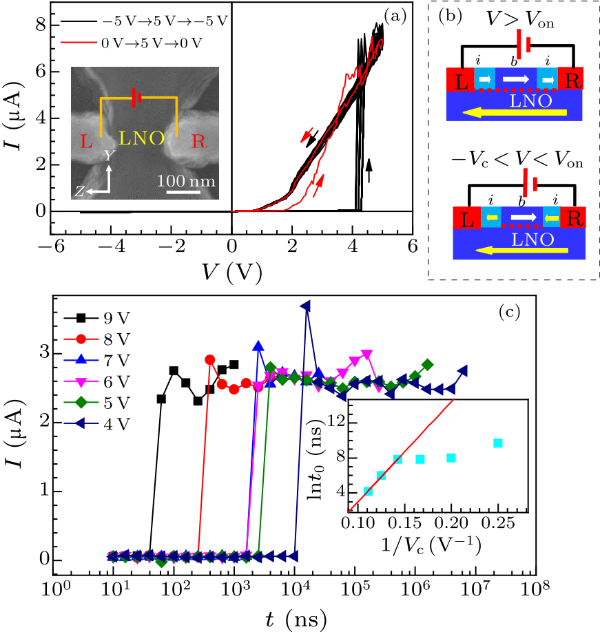
Fig. 1. (a) Double $I$–$V$ curves of 100 sweeps (black lines) between $-5$ V and 5 V for an LNO cell with dimensions of $w\times l\times h = 105\times 138\times 120$ nm$^{3}$. The red line shows the on-state $I$–$V$ curve after poling at 5 V, and the inset shows the SEM image of the cell in contact with L and R electrodes. The thin arrows indicate the voltage sweeping directions. (b) The orientations (thick arrows) of interfacial domains (${i}$) and inner domains (${b}$) under different applied voltages for the above LNO nanodevice after poling at 5 V, where the dotted lines show the DWs. (c) Switching time dependence of wall current at 3 V for different switching voltages, where the inset shows the ln$t_{0}$–$1/V$ plot, fitted by a solid line.
Figure 1(a) shows 100 sweeps of $I$–$V$ curves between $-5$ V and 5 V (black lines) for an LNO cell with dimensions of $w\times l\times h = 105\times 138\times 120$ nm$^{3}$ (see the SEM photograph in the inset). The initial OFF current jumps to an ON current of 5.8 µA above a positive coercive voltage ($V_{\rm c}$) of 4.2 V. The ON current flows through the conducting DW path formed between the switched domain within the entire cell and the unswitched domain at the bottom.[18,22] The loops are highly stable against the sweeping cycles, with less dispersion than other defect-mediated resistance switching.[20,21,23] Following device poling at 5 V, a repeated $I$–$V$ sweep between 0 and 5 V shows a diode-like on-state DW current that turns on above an onset voltage ($V_{\rm on}$) of 2.0 V (red line, $V_{\rm on} < V_{\rm c}$). The diode-like DW current is rectified by the interfacial domains ($i$) near the L and R electrodes, which then revert to their initial orientations to erase the interfacial DWs as $V < V_{\rm on}$ due to the built-in interfacial imprint fields, in contrast to the inner nonvolatile DWs ($b$), as illustrated by the sketches in Fig. 1(b).[18] As $V > V_{\rm on}$, the interfacial domains are switched again along the electric field direction, and the ON current appears. The volatile nature of the two interfacial domains can be determined via high-resolution transmission electron microscopy observations, for thicknesses of 7.2 nm and 3.6 nm, respectively.[18] In addition, line scans of the Nb–N$_{2,3}$, Li–K, Nb–M$_{4,5}$ and O–K edges of the electron energy loss spectroscopy (EELS) spectrum in LNO quantify the Li/Nb atomic ratio as varying from 0.72 to 0.97 within the interfacial-layer thickness, indicating the presence of a Li deficiency. An imprint field is built up by the gradient distribution of the Li deficiency, and backswitches the $i$ domains during the relaxation period.[18] The inner 180$^{\circ}$ DWs generally have small inclination angles ($\sim$$1^{\circ}$) and local sideways meandering behavior, which contains the charged dipoles,[8] thereby demonstrating characteristic n-type conduction.[22] Figure 1(c) shows the domain switching time ($t$) dependence of the on-current at 3 V for a cell, based on the application of various switching voltages. The current jumps abruptly from the off-state to the on-state at the characteristic domain switching time $t_{0}$. Based on the Merz law, we obtain the equation $$ V_{\rm c} =\frac{V_{\rm a} }{\ln t_{0} -\ln \tau_{0} },~~ \tag {1} $$ where $\tau_{0}$ is the ultimate dipole flipping time of $\sim $200 fs,[24] and $V_{\rm a}$ is the activation voltage. The inset in Fig. 1(c) shows the $\ln t_{0}$–$1/V_{\rm c}$ plot fitted by a solid line, in accordance with Eq. (1), from which we estimated $V_{\rm a}$ to be 115 V. However, the fit is unsuccessful, as $V_{\rm c} \le 6$ V, where the domain switching dynamics change. For an input bipolar sine wave at a frequency of 1/2$t_{0}$, the ON current would appear when $V > V_{\rm c}(t_{0})$, but turn off when $V < 0$ for the realization of half-wave rectification. Figure 2(a) shows the output wall current transients (lower panel) from an LNO cell under input sine waves at frequencies of 10 Hz for different amplitudes (upper panel). The half-wave rectified ON currents appear when $V \ge 4$ V ($\sim$$V_{\rm c}$), but disappear when $V \le 3.8$ V. This capacity for current rectification and adjustable cut-off voltage ($V_{\rm c} \propto l$) is useful for the power protection and voltage stabilization of the nanodevices in the circuits. For the realization of full-wave rectification, two parallel diodes in opposite voltage polarities are suggested in Fig. 2(b), as illustrated by a bipolar $I$–$V$ curve.
cpl-38-1-017701-fig2.png
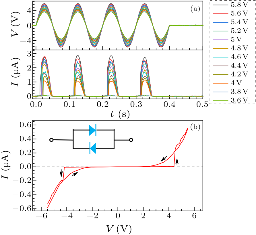
Fig. 2. (a) Output wall current transients (lower panel) from an LNO cell with dimensions of $w\times l\times h = 105\times 138\times 120$ nm$^{3}$, based on input sine waves at a frequency of 10 Hz at different amplitudes (upper panel). (b) The double $I$–$V$ curve for two identical LNO cells with dimensions of $w\times l\times h = 117\times 56\times 45$ nm$^{3}$, connected in opposite diode polarities, as shown by equivalent circuit diagram in the inset. The arrows indicate voltage sweeping directions.
cpl-38-1-017701-fig3.png
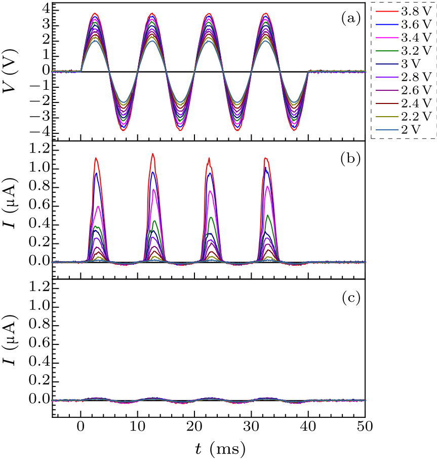
Fig. 3. (a) Input sine waves at a frequency of 100 Hz for different amplitudes. (b) Output wall current transients from an LNO cell with dimensions of $w\times l\times h = 105\times 138\times 120$ nm$^{3}$ after poling at 5 V. (c) Output wall current transients from the cell after poling at $-5$ V.
The half-wave ON currents at voltages between $V_{\rm on}$ and $V_{\rm c}$ are dependent on domain orientations. Figures 3(a) shows the input sine waves for different amplitudes at a frequency of 100 Hz. Figure 3(b) shows the output half-wave ON current transients from a nanodevice poled at 5 V, where the cut-off voltage is reduced from the previous $V_{\rm c}$ [4 V in Fig. 2(a)] to $V_{\rm on}$ [2 V in Fig. 3(b)]. Once the device is poled at an opposite voltage of $-5$ V, the ON currents turned off completely, due to DW erasure, as shown in Fig. 3(c). Therefore, the diode can be repeatedly created and deleted in the circuit. With a combination of two parallel diodes in opposite polarities, as shown in Fig. 2(b), it is possible to conveniently change the diode polarity between $V_{\rm on}$ and $V_{\rm c}$ in the circuit using two opposite poling voltages of $+$/$-$5 V, in addition to the achievement of full-wave rectification. This redefinition and erasable quality in nano-diodes cannot be realized by traditional semiconductors using p–n junctions. Figure 4 shows output wall current transients from an LNO cell after poling at 5 V for various input sine waves at different frequencies, and at an amplitude of 3.8 V. The output half-wave ON current reduces a little with increasing frequency, before rapidly attenuating at 5 kHz. This damping effect is due to frequency-dependent $V_{\rm on}$ enlargement in the interfacial domains, analogous to the $V_{\rm c}-t_{0}$ dependence described by Eq. (1). Theoretically, the time can shorten to the ns-to-ps order of magnitude with enhanced applied electric field strength,[24] which is suitable for application in microwave devices at gigahertz frequencies.[25]
cpl-38-1-017701-fig4.png
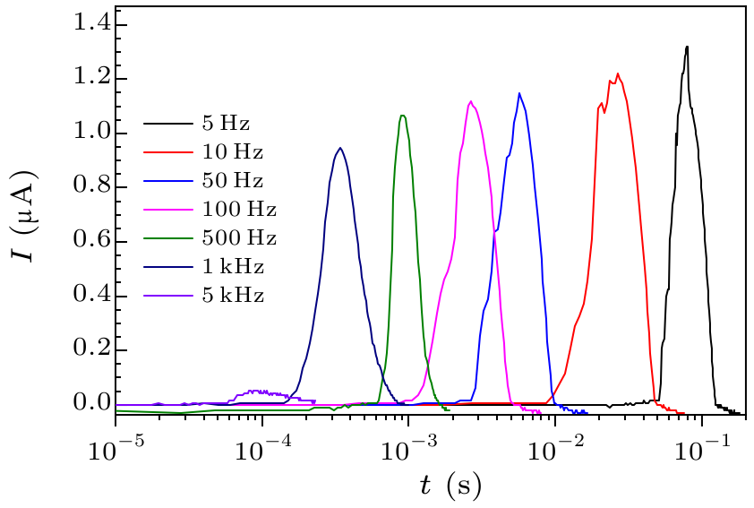
Fig. 4. (a) Output wall current transients at different frequencies for various input sine waves in amplitudes of 3.8 V from an LNO cell with dimensions of $w\times l\times h = 105\times 138\times 120$ nm$^{3}$ after poling at 5 V.
In conclusion, the diode-like wall current across the LNO cell can be used for half-wave and full-wave rectification with the application of bipolar sine waves in amplitudes, either above $V_{\rm c}$, or between $V_{\rm on}$ and $V_{\rm c}$. For the latter, the half-wave ON currents, which depend on domain orientations, can be turned on/off for a nanodevice poled at $+$/$-$5 V, respectively. With the parallel connection of two diodes in opposite polarities in the circuit, it is possible to change the diode polarity via the simultaneous selection of one cell as achieving full-wave rectification. Finally, we found that both $V_{\rm c}$ and $V_{\rm on}$ varied with the input wave frequency, in accordance with the Merz law. These erasable domain wall diodes can potentially provide active elements for future nano-electronic devices.
References Nonvolatile ferroelectric domain wall memoryTemporary formation of highly conducting domain walls for non-destructive read-out of ferroelectric domain-wall resistance switching memoriesConduction at domain walls in oxide multiferroicsConduction through 71° Domain Walls in BiFeO 3 Thin FilmsPolarization charge as a reconfigurable quasi-dopant in ferroelectric thin filmsConduction of Topologically Protected Charged Ferroelectric Domain WallsAnisotropic conductance at improper ferroelectric domain wallsConducting Domain Walls in Lithium Niobate Single CrystalsEnhancing the Domain Wall Conductivity in Lithium Niobate Single CrystalsLarge and accessible conductivity of charged domain walls in lithium niobateFree-electron gas at charged domain walls in insulating BaTiO3Domain-wall conduction in AFM-written domain patterns in ion-sliced LiNbO 3 filmsControllable conductive readout in self-assembled, topologically confined ferroelectric domain wallsHierarchical Domain Structure and Extremely Large Wall Current in Epitaxial BiFeO 3 Thin FilmsPersistent conductive footprints of 109° domain walls in bismuth ferrite filmsDomain-wall conduction in ferroelectric BiFeO3 controlled by accumulation of charged defectsGiant Domain Wall Conductivity in Self‐Assembled BiFeO 3 NanocrystalsFerroelectric domain wall memory with embedded selector realized in LiNbO3 single crystals integrated on Si wafersEnergy-Efficient Ferroelectric Domain Wall Memory with Controlled Domain Switching DynamicsDouble-Layer-Stacked One Diode-One Resistive Switching Memory Crossbar Array with an Extremely High Rectification Ratio of 10 9High-Performance and Low-Power Rewritable SiO x 1 kbit One Diode-One Resistor Crossbar Memory ArrayNonvolatile ferroelectric field-effect transistorsResistive switching materials for information processingUnderstanding the Nature of Ultrafast Polarization Dynamics of Ferroelectric Memory in the Multiferroic BiFeO 3Microwave a.c. conductivity of domain walls in ferroelectric thin films
[1] Sharma P, Zhang Q, Sando D, Lei C H, Liu Y, Li J, Nagarajan V and Seidel J 2017 Sci. Adv. 3 e1700512
[2] Jiang J, Bai Z L, Chen Z H, He L, Zhang D W, Zhang Q H, Shi J A, Park M H, Scott J F, Hwang C S and Jiang A Q 2018 Nat. Mater. 17 49
[3] Seidel J, Martin L W, He Q, Zhang Q, Chu Y H, Rother A, Hawkridge M E, Maksymovych P, Yu P, Gajek M, Balke N, Kalinin S V, Gemming S, Wang F, Catalan G, Scott J F, Spaldin N A, Orenstein J and Ramesh R 2009 Nat. Mater. 8 229
[4] Farokhipoor S and Noheda B 2011 Phys. Rev. Lett. 107 127601
[5] Crassous A, Sluka T, Tagantsev A K and Setter N 2015 Nat. Nanotechnol. 10 614
[6] Wu W, Horibe Y, Lee N, Cheong S W and Guest J R 2012 Phys. Rev. Lett. 108 077203
[7] Meier D, Seidel J, Cano A, Delaney K, Kumagai Y, Mostovoy M, Spaldin N A, Ramesh R and Fiebig M 2012 Nat. Mater. 11 284
[8] Schröder M, Hau M A, Thiessen A, Soergel E, Woike T and Eng L M 2012 Adv. Funct. Mater. 22 3936
[9] Godau C, Kämpfe T, Thiessen A, Eng L M and Haußmann A 2017 ACS Nano 11 4816
[10] Werner C S, Herr S J, Buse K, Sturman B, Soergel E, Razzaghi C and Breunig I 2017 Sci. Rep. 7 9862
[11] Sluka T, Tagantsev A K, Bednyakov P and Setter N 2013 Nat. Commun. 4 1808
[12] Volk T R, Gainutdinov R V and Zhang H H 2017 Appl. Phys. Lett. 110 132905
[13] Ma J, Zhang Q, Peng R, Wang J, Liu C, Wang M, Li N, Chen M, Cheng X, Gao P, Gu L, Chen L Q, Yu P, Zhang J and Nan C W 2018 Nat. Nanotechnol. 13 947
[14] Bai Z L, Cheng X X, Chen D F, Zhang D W, Chen L Q, Scott J F, Hwang C S and Jiang A Q 2018 Adv. Funct. Mater. 28 1801725
[15] Stolichnov I, Iwanowska M, Colla E, Ziegler B, Gaponenko I, Paruch P, Huijben M, Rijnders G and Setter N 2014 Appl. Phys. Lett. 104 132902
[16] Rojac T, Bencan A, Drazic G, Sakamoto N, Ursic H, Jancar B, Tavcar G, Makarovic M, Walker J, Malic B and Damjanovic D 2017 Nat. Mater. 16 322
[17] Liu L, Xu K, Li Q, Daniels J, Zhou H, Li J, Zhu J, Seidel J and Li J F 2020 Adv. Funct. Mater. 2005876
[18] Jiang A Q, Geng W P, Lv P, Hong J W, Jiang J, Wang C, Chai X J, Lian J W, Zhang Y, Huang R, Zhang D W, Scott J F and Hwang C S 2020 Nat. Mater. 19 1188
[19] Wang C, Jiang J, Chai X, Lian J, Hu X and Jiang A Q 2020 ACS Appl. Mater. & Interfaces 12 44998
[20] Yoon K J, Kim G H, Yoo S, Bae W, Yoon J H, Park T H, Kwon D E, Kwon Y J, Kim H J and Kim Y M 2017 Adv. Electron. Mater. 3 1700152
[21] Wang G, Lauchner A C, Lin J, Natelson D, Palem K V and Tour J M 2013 Adv. Mater. 25 4789
[22] Chai X J, Jiang J, Zhang Q H, Hou X, Meng F Q, Wang J, Gu L, Zhang D W and Jiang A Q 2020 Nat. Commun. 11 2811
[23] Wang Z R, Wu H Q, Burr G W, Hwang C S, Wang K L, Xia Q F and Yang J J 2020 Nat. Rev. Mater. 5 173
[24] R, D S, Kawayama I, Mavani K, Takahashi K, Murakami H and Tonouchi M 2009 Adv. Mater. 21 2881
[25] Tselev A, Yu P, Cao Y, Dedon L R, Martin L W, Kalinin S V and Maksymovych P 2016 Nat. Commun. 7 11630