Chinese Physics Letters, 2020, Vol. 37, No. 6, Article code 068503 A Novel Oxygen-Based Digital Etching Technique for p-GaN/AlGaN Structures without Etch-Stop Layers * Yang Jiang (蒋洋)1, Ze-Yu Wan (万泽宇)2, Guang-Nan Zhou (周广楠)1, Meng-Ya Fan (范梦雅)1, Gai-Ying Yang (杨改英)1,5, R. Sokolovskij1, Guang-Rui Xia (夏光睿)1,2, Qing Wang (汪青)1,3,6**, Hong-Yu Yu (于洪宇)1,4,6** Affiliations 1School of Microelectronics, Southern University of Science and Technology, Shenzhen 518055, China 2Department of Materials Engineering, The University of British Columbia, Vancouver, British Columbia V6T 1Z4, Canada 3Dongguan Institute of Opto-Electronics Peking University, Dongguan 523808, China 4Engineering Research Center of Integrated Circuits for Next-Generation Communications (Ministry of Education), Shenzhen 518055, China 5School of Innovation & Entrepreneurship, Southern University of Science and Technology, Shenzhen 518055, China 6Shenzhen Institute of the Third Generation Semiconductor, Shenzhen 518100, China Received 7 March 2020, online 26 May 2020 *Supported by the Guangdong Science and Technology Department (Grant Nos. 2019B010128001 and 2019B010142001), the Shenzhen Municipal Council of Science and Innovation (Grant Nos. JCYJ20180305180619573 and JCYJ20170412153356899), and the National Natural Science Foundation of China (Grant No. 61704004).
**Corresponding authors. Email: wangq7@sustech.edu.cn; yuhy@sustech.edu.cn
Citation Text: Jiang Y, Wan Z Y, Zhou G N, Fan M Y and Yang G Y et al 2020 Chin. Phys. Lett. 37 068503    Abstract A novel O$_{2}$ plasma-based digital etching technology for p-GaN/AlGaN structures without any etch-stop layer was investigated using an inductively coupled plasma (ICP) etcher, with 100 W ICP power and 40 W rf bias power. Under 40 sccm O$_{2}$ flow and 3 min oxidation time, the p-GaN etch depth was 3.62 nm per circle. The surface roughness improved from 0.499 to 0.452 nm after digital etching, meaning that no observable damages were caused by this process. Compared to the dry etch only methods with Cl$_{2}$/Ar/O$_{2}$ or BCl$_{3}$/SF$_{6}$ plasma, this technique smoothed the surface and could efficiently control the etch depth due to its self-limiting characteristic. Furthermore, compared to other digital etching processes with an etch-stop layer, this approach was performed using ICP etcher and less demanding on the epitaxial growth. It was proved to be effective in precisely controlling p-GaN etch depth and surface damages required for high performance p-GaN gate high electron mobility transistors. DOI:10.1088/0256-307X/37/6/068503 PACS:85.30.De, 81.05.Ea, 68.37.Lp, 68.37.Ps © 2020 Chinese Physics Society Article Text Compared to the conventional Si-based high-power devices, GaN-based high electron mobility transistors (HEMTs) have many excellent properties such as high breakdown voltage, high electron mobility and high saturation electron velocity.[1–3] E-mode GaN HEMTs have attracted much attention due to their low power assumption and simple circuit design.[2–4] Several techniques have been developed for E-mode GaN HEMTs, such as gate recess,[5] fluoride ion implantation,[6,7] and p-GaN cap layer.[8,9] The fluoride ion implantation and gate recess approaches could cause poor process repeatability and severe reliability problems.[10,11] Researchers have taken p-GaN gate HEMTs as the most promising technology for E-mode devices because of their outstanding device performance and industrial prospects. Two major challenges for the fabrication of high-performance p-GaN gate HEMTs are etching uniformity and plasma damages.[12,13] The dry etch only approach with chlorine (Cl$_{2}$) or boron trichloride (BCl$_{3}$) plasma has high etch rate. However, it could cause lots of surface damages to the underlying AlGaN layer.[14] Additionally, the etch depth is controlled by the etching time, which could easily cause under-etching or over-etching problems. Several high selectivity ICP etching methods for p-GaN/AlGaN structures with Cl$_{2}$/O$_{2}$/N$_{2}$ or BCl$_{3}$/SF$_{6}$ plasmas have been reported to improve etching uniformity and to reduce etching damages.[15,16] Nevertheless, they suffer from poor technical repeatability. Digital etching was to achieve a specified etch depth by consecutive repetitions of a two-step process. On the first step the GaN epitaxial layer was oxidized through oxygen plasma treatment, wet oxidation, electrochemical oxidation or thermal oxidation methods. On the second step the so-formed oxide is selectively removed using dry or wet etching, with negligible effect on the underlying un-oxidized material.[17] Digital etching process was developed to accurately control etch depth and to improve surface morphology by its self-limiting characteristic. Buttari et al.[17] proposed a digital etching technique for AlGaN/GaN HEMTs using a dry plasma etching step and a wet etching step to remove 5–6 Å AlGaN in a two-step etching circle, but the etch rate was very low. Burnham et al.[18] demonstrated a new O$_{2}$-BCl$_{3}$ digital etching technique for gate-recess GaN-on-Si HEMTs using atomic layer etching. Using N$_{2}$O oxidizing agent with reactive ion etching and HCl wet etching, Chiu et al.[13,19] realized p-GaN gate HEMTs. In their work, 1 nm AlN layer under p-GaN was applied as an etch-stop layer to achieve self-terminated digital etching. A new digital etching process using O$_{2}$ plasma with ICP-RIE plasma oxidation and HCl wet etching for AlGaN/GaN was reported by Sokolovskij et al.[20] In this work, we report a digital etching method without any etch-stop layer for p-GaN gate E-mode HEMTs, which combines an ICP oxidation step with O$_{2}$ plasma and a HCl wet etching step. The p-GaN etch depth and surface roughness is measured with an atomic force microscope (AFM). Furthermore, the mechanism of this etching process is analyzed by x-ray photoelectron spectroscopy (XPS) and scanning transmission electron microscopy (STEM) attached with energy dispersive x-ray spectroscopy (EDX), shown to be effective to precisely control the p-GaN etch depth and to smooth the surface due to the self-limiting characteristic. The p-GaN/AlGaN epi wafers in this work were grown by Enkris Semiconductor Inc. The schematic and STEM cross-section photograph of p-GaN/AlGaN wafer were shown in Fig. 1. Au protect layer for STEM measurement was deposited by sputter coater, which could not cause any structural/composition change on p-GaN surface.
cpl-37-6-068503-fig1.png
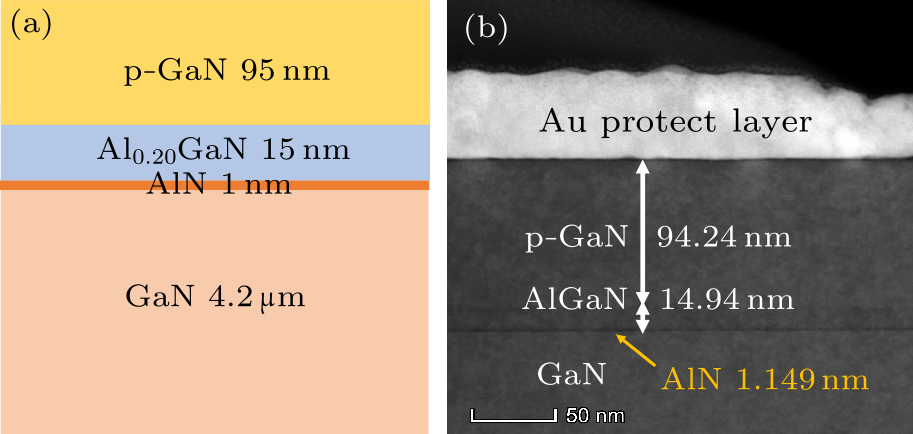
Fig. 1. (a) Schematic cross sections and (b) STEM image of the top epitaxy layers of p-GaN/AlGaN wafer.
cpl-37-6-068503-fig2.png
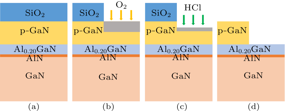
Fig. 2. Schematic diagrams showing the cross sections of the epitaxy structure during the whole etching process: (a) SiO$_{2}$ deposition as hard mask, (b) ICP plasma oxidation, (c) HCl wet etching, (d) SiO$_{2}$ hard mask removal after p-GaN etching.
A 300 nm SiO$_{2}$ layer deposited by plasma enhanced chemical vapor deposition (PECVD) was used as the hard mask for ICP plasma oxidation (Fig. 2(a)). Then the pattern of hard mask was defined by photolithography and ICP etching with SF$_{6}$ plasma. Each digital etching cycle includes the two steps shown in Figs. 2(b) and 2(c). The first step was to oxidize p-GaN by O$_{2}$ plasma with an ICP etcher in which the chamber pressure was maintained at 15 mTorr in order to improve the etching uniformity. A series of experiments was carried out with different O$_{2}$ flows, rf power, ICP power and oxidation time (Fig. 3). In the wet etch steps, a 3-min etch step in a diluted HCl solution (deionized water: HCl = $4\!:\!1$) was used. After the whole digital etching process, the SiO$_{2}$ layer was removed by buffered oxide etch (BOE) (Fig. 2(d)).
cpl-37-6-068503-fig3.png
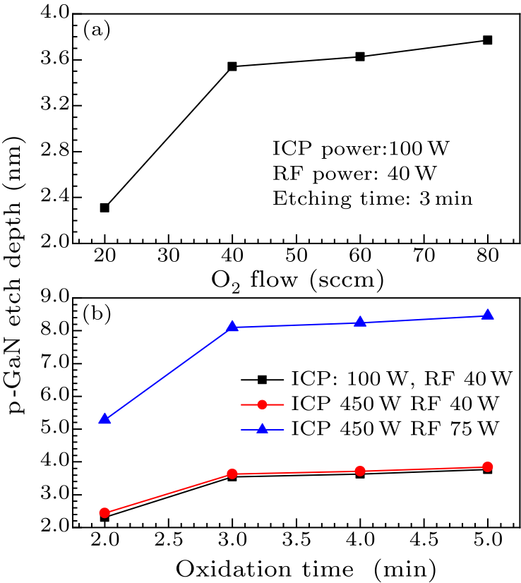
Fig. 3. (a) Characteristics of p-GaN etch depth under different O$_{2}$ flow, (b) p-GaN etch depth under different ICP power and rf power at 40 sccm O$_{2}$ flow.
According to the theories of digital etching,[2,20] p-GaN oxidation depth was self-limited under different O$_{2}$ flows and oxidation time for each digital etching circle. Figure 3(a) demonstrates that p-GaN etch depth was not substantially increased when the O$_{2}$ flow was higher than 40 sccm, which could be attributed to the fact that the concentration of O$_{2}$ plasma was saturated at 100 W ICP power, 40 W rf power and 40 sccm O$_{2}$ flow. We selected 40 sccm O$_{2}$ flow and 3 min oxidation time because of its good process repeatability. Several experiments with different ICP and rf power settings were performed (Fig. 3(b)). When the concentration of O$_{2}$ plasma was set at 40 sccm, the p-GaN etch depth remained almost unchanged with ICP power increasing from 100 W to 450 W, however, O$_{2}$ plasma could further penetrate into p-GaN layer by increasing rf power, inducing the increase in the p-GaN etch depth. It is demonstrated that p-GaN etch depth mainly depended on rf power.[20] Taking the surface morphology and plasma damage into consideration, the optimized recipe with 100 W ICP power and 40 W rf power was chosen. The p-GaN etch depth per cycle measured by AFM was 3.62 nm. The surface morphology of p-GaN/AlGaN wafer before and after the digital etching process was measured by AFM with a scan area of $1 \times 1$ µm$^{2}$ (Fig. 4). The rms roughness and mean roughness are listed in Table 1. The rms roughness increased to 0.529 nm and 0.573 nm for the Cl$_{2}$/Ar/O$_{2}$ and BCl$_{3}$/SF$_{6}$ etching samples, respectively. However, after digital etching, the rms roughness decreased slightly from 0.499 nm to 0.452 nm, suggesting that this technique smoothed the surface. The smoothed surface was attributed to the fact that the O$_{2}$ plasma bombardment in ICP oxidation process was mainly performed on Ga$_{2}$O$_{3}$ surface layer, with negligible effect on the underlying un-oxidized p-GaN layer. It was demonstrated that this digital etching technique was an efficient way to control p-GaN etch depth and surface damages, which could consequently improve the ohmic contact and output characteristics of the p-GaN E-mode HEMTs.
cpl-37-6-068503-fig4.png
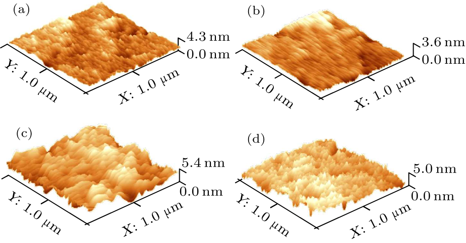
Fig. 4. AFM images of p-GaN surface: (a) as-grown, (b) after one circle digital etching, (c) after Cl$_{2}$/Ar/O$_{2}$ etching, (d) after BCl$_{3}$/SF$_{6}$ etching.
Table 1. Surface roughness measured by AFM of p-GaN layer: as-grown, after digital etching, after Cl$_{2}$/Ar/O$_{2}$ etching and after BCl$_{3}$/SF$_{6}$ etching.
Etching method rms roughness Mean roughness
(nm) (nm)
As grown 0.499 0.383
Digital etching 0.452 0.351
Cl$_{2}$/Ar/O$_{2}$ etching 0.529 0.406
BCl$_{3}$/SF$_{6}$ etching 0.573 0.436
cpl-37-6-068503-fig5.png
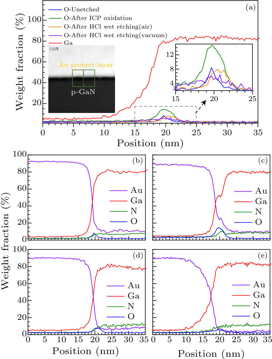
Fig. 5. The EDX analysis in the Au/p-GaN interface (a) O$_{2}$ weight fraction variation during whole process, STEM image showing EDX line scan area (green box and arrow), (b) as-grown and exposed in air, (c) after ICP plasma oxidation, (d) after ICP plasma oxidation, followed by HCl wet etching and exposed to air, (e) after ICP plasma oxidation, followed by HCl wet etching and sealing in vacuum.
cpl-37-6-068503-fig6.png
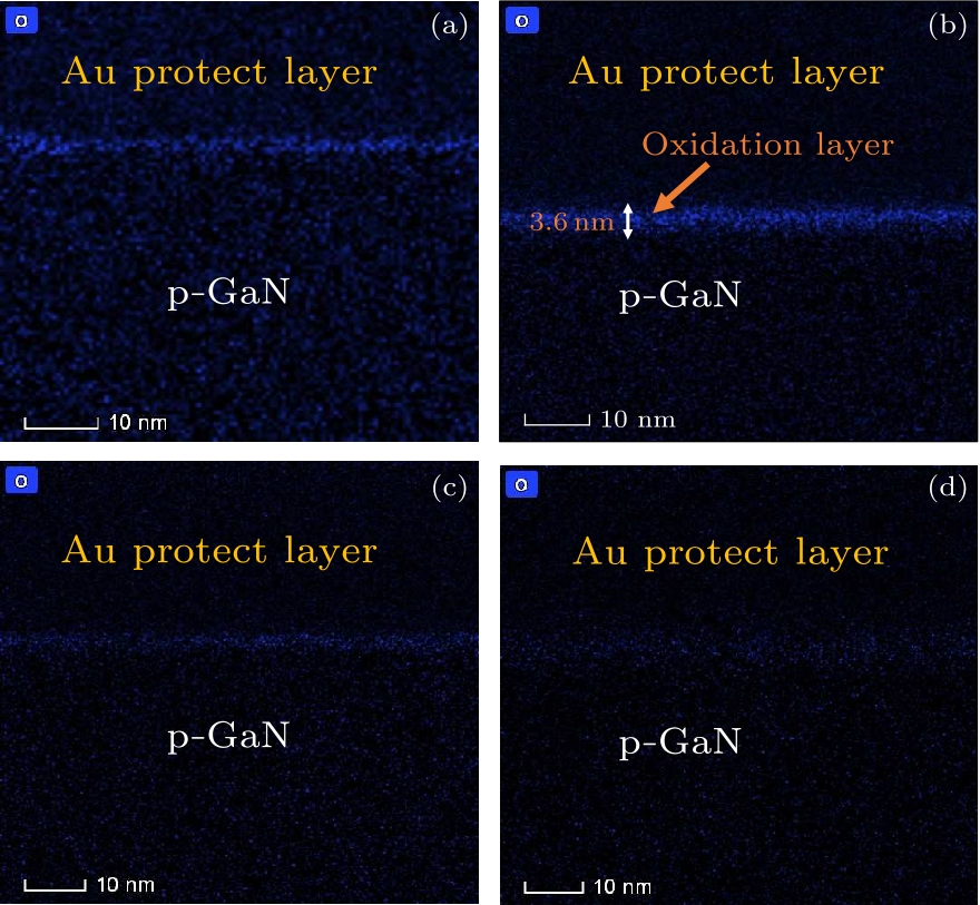
Fig. 6. STEM/EDX mapping showing O$_2$ element distribution at p-GaN surface: (a) as-grown and exposed in air, (b) after ICP plasma oxidation, (c) after ICP plasma oxidation, followed by HCl wet etching and exposed to air, (d) after ICP plasma oxidation, followed by HCl wet etching and sealing in vacuum.
cpl-37-6-068503-fig7.png
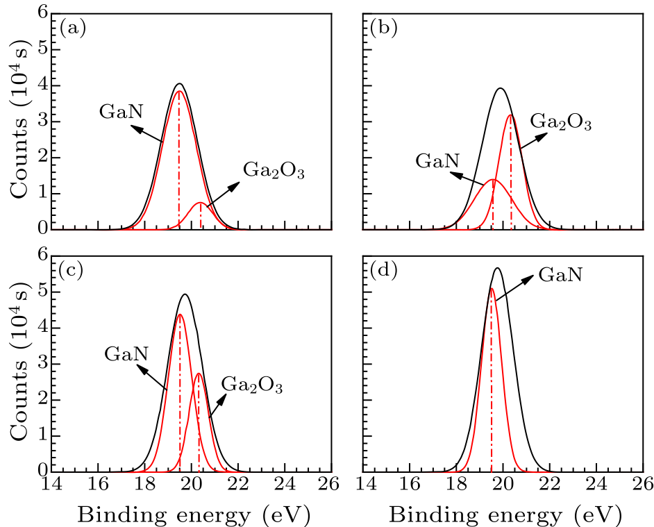
Fig. 7. XPS measurements of samples: (a) as-grown and exposed in air, (b) after ICP plasma oxidation, (c) after ICP plasma oxidation, followed by HCl wet etching and exposed to air, (d) after ICP plasma oxidation, followed by HCl wet etching and sealing in vacuum.
STEM/EDX and XPS were used to study the element distribution and compound content of the p-GaN surface layer. A typical STEM image of EDX line scan area is shown in Fig. 5(a). The image was obtained by a well tilted TEM sample to present the epi layers clearly. The inset in Fig. 5(a) reveals clearly the presence of an oxide layer in the sample by only ICP oxidation. Figures 5(b)–5(e) demonstrate the element weight fraction at the p-GaN surface layer by EDX for the samples with different etching processes. The weight fraction of oxygen at the surface increased from 8.39% to 14.62% after ICP plasma oxidation, implying that a thicker oxidation layer was formed at the p-GaN surface. Furthermore, the thickness of oxidation layer was 3.6 nm, which matched well with the p-GaN etch depth per circle measured by AFM (Fig. 6(b)). After removing the oxidation layer by HCl solution and followed by exposing to air, the oxygen weight fraction dropped to the same level as the unetched p-GaN sample. For the HCl etched sample followed by immediate vacuum sealing, oxygen was almost negligible at the surface. In Fig. 6, we can clearly see the variation of the oxidation layer during the etching process. We propose that p-GaN was firstly oxidized to Ga$_{2}$O$_{3}$, which could be selectively removed by HCl solution in the following wet etch step.[20] This assumption was further confirmed by XPS measurement shown in Fig. 7. Based on the results of EDX and XPS, to explain the digital etching process we give $$\begin{align} &{\rm GaN}+{\rm O}_{2}\to {\rm Ga}_{2}{\rm O}_{3}+{\rm N}_{2},~~ \tag {1} \end{align} $$ $$\begin{align} &{\rm Ga}_{2}{\rm O}_{3}+{\rm HCl}\to {\rm GaCl}_{3}+{\rm H}_{2}{\rm O}.~~ \tag {2} \end{align} $$ In summary, we have investigated O$_{2}$ plasma-based digital etching of p-GaN/AlGaN structures without any etch-stop layer using inductively coupled plasma (ICP) etcher for the preparation of p-GaN gate E-mode HEMTs. Under 40 sccm O$_{2}$ flow and 3 min oxidation time, the p-GaN etch depth is 3.62 nm per circle. The surface roughness is improved from 0.499 to 0.452 nm after digital etching, meaning that no observable damage is caused by this process. Compared to the rms roughness of 0.529 nm and 0.573 nm for Cl$_{2}$/Ar/O$_{2}$ and BCl$_{3}$/SF$_{6}$ etching process, this technique smooths the surface. Compared to other digital etching processes with an etch-stop layer, this approach is performed using ICP etcher and less demanding on the epitaxial growth. XPS and TEM results suggest that p-GaN is firstly oxidized to Ga$_{2}$O$_{3}$ and consequently removed by HCl solution. The technique is proved to be effective in precisely controlling p-GaN etch depth and surface damages required for high-performance p-GaN gate high electron mobility transistors.
References Precise thickness control in recess etching of AlGaN/GaN hetero-structure using photocarrier-regulated electrochemical processEnhancement-mode AlGaN/GaN HEMT and MIS-HEMT technologyCl[sub 2] reactive ion etching for gate recessing of AlGaN/GaN field-effect transistorsOrigin of etch delay time in Cl2 dry etching of AlGaN/GaN structuresAlGaN/GaN Recessed MIS-Gate HFET With High-Threshold-Voltage Normally-Off Operation for Power Electronics Applications6.5 V High Threshold Voltage AlGaN/GaN Power Metal-Insulator-Semiconductor High Electron Mobility Transistor Using Multilayer Fluorinated Gate StackEffect of very low power inductively coupled plasma etching on ohmic contacts to p-GaNGaN-on-Si Power Technology: Devices and ApplicationsNegative transconductance effect in p-GaN gate AlGaN/GaN HEMTs by traps in unintentionally doped GaN buffer layerStudy of fluorine bombardment on the electrical properties of AlGaN∕GaN heterostructuresReliability of Enhancement-mode AlGaN/GaN HEMTs Fabricated by Fluorine Plasma TreatmentProperties of p-type GaN etched by inductively coupled plasma and their improvementHigh Uniformity Normally-OFF p-GaN Gate HEMT Using Self-Terminated Digital Etching TechniqueRecessed-Gate Enhancement-Mode AlGaN/GaN Heterostructure Field-Effect Transistors on Si with Record DC Performancep-GaN Gate Enhancement-Mode HEMT Through a High Tolerance Self-Terminated Etching ProcessSELECTIVE DRY ETCHING OF GaN OVER AlGaN IN BCL 3 / SF 6 MIXTURESDigital etching for highly reproducible low damage gate recessing on AlGaN/GaN HEMTsGate-recessed normally-off GaN-on- Si HEMT using a new O2-BCl3 digital etching techniqueCharacterization of enhancement-mode AlGaN/GaN high electron mobility transistor using N 2 O plasma oxidation technologyPrecision Recess of AlGaN/GaN with Controllable Etching Rate Using ICP-RIE Oxidation and Wet Etching
[1] Yusuke K, Keisuke U, Taketomo S, Tamotsu H et al 2017 J. Appl. Phys. 121 184501
[2] Chen K, Zhou C et al 2011 Phys. Status Solidi A 208 434
[3] Chen C, Keller S, Haberer E, Zhang L, Hu S E, Mishra U, Wu Y et al 1999 J. Vac. Sci. & Technol. B 17 2755
[4] Buttari D et al 2003 Appl. Phys. Lett. 83 4779
[5] Oka T et al 2008 IEEE Electron Device Lett. 29 668
[6] Wang Y H et al 2015 IEEE Electron Device Lett. 36 381
[7] Baharin A et al 2010 Conference on Optoelectronic and Microelectronic Materials and Devices (Canberra, ACT, Australia 12–15 December 2010) p 145
[8] Chen K J et al 2017 IEEE Trans. Electron Devices 64 779
[9] Ge M, Cai Q, Zhang B H et al 2019 Chin. Phys. B 28 107301
[10] Basu A, Kumar V, Adesida I et al 2007 J. Vac. Sci. & Technol. B 25 2607
[11] Yi C W, Wang R N, Huang W et al 2007 IEEE International Electron Devices Meeting (Washington DC, USA 10–12 December 2007) p 389
[12] Lv L, Gong X, Hao Y et al 2008 Acta Phys. Sin. 57 1128 (in Chinese)
[13] Chiu H C et al 2018 IEEE Trans. Electron Devices 65 4820
[14] Hahn H, Lükens G, Ketteniss N et al 2011 Appl. Phys. Express 4 114102
[15] Zhou Y, Zhong Y Z, Gao H W et al 2017 IEEE J. Electron Devices Soc. 5 340
[16] Buttari D, Chini A, Chakraborty A, Mishra U K et al 2004 Int. J. High Speed Electron. Syst. 14 756
[17] Buttari D, Heikman S, Keller S et al 2002 IEEE Lester Eastman Conference on High Performance Devices (Newark, DE, USA 6–8 August 2002) p 461
[18] Burnham S, Boutros K, Hashimoto P, Butler C, Wong D, Hu M, Micovic M et al 2010 Phys. Status Solidi C 7 2010
[19] Chiu H C, Yang C W, Chen C H, Fu J S, Chen F T et al 2011 Appl. Phys. Lett. 99 153508
[20] Sokolovskij R, Sun J, Santagata F, Iervolino E, Li S, Zhang G Y, Sarro P M, Zhang G Q et al 2016 Procedia Eng. 168 1094