Chinese Physics Letters, 2019, Vol. 36, No. 12, Article code 127301Express Letter The Unconventional Influence of a Nearby Molecule onto Transport of Single C$_{60}$ Molecule Transistor * Xiao Guo (郭潇)1,2, Wen-jie Liang (梁文杰)1,2,3** Affiliations 1Beijing National Center for Condensed Matter Physics, Beijing Key Laboratory for Nanomaterials and Nanodevices, Institute of Physics, Chinese Academy of Sciences, Beijing 100190 2CAS Center of Excellence in Topological Quantum Computation and School of Physical Sciences, University of Chinese Academy of Sciences, Beijing 100190 3Songshan Lake Materials Laboratory, Dongguan 523808 Received 18 October 2019, online 05 November 2019 *Supported by the National Key R&D Program of China (2016YFA0200800), the Strategic Priority Research Program of Chinese Academy of Sciences under Grant Nos XDB30000000 and XDB07030100, the Sinopec Innovation Scheme (A-381), and the Rise-Sinopec Fund (No 10010104-18-ZC0609-0003).
**Corresponding author. Email: wjliang@iphy.ac.cn
Citation Text: Guo X and Liang W J 2019 Chin. Phys. Lett. 36 127301    Abstract We study the transport property of single C$_{60}$ molecular transistors with special focus on the situation that other molecules are in vicinity. The devices are prepared using electromigration and thermal deposition techniques. Pure single C$_{60}$ molecule transistors show typical coulomb blockade behavior at low temperature. When we increase the coverage of molecules slightly by extending the deposition time, the transport spectrum of devices displays a switching behavior in the general coulomb blockade pattern. We attribute this unconventional phenomenon to the influence from a nearby C$_{60}$ molecule. By analyzing this transport behavior quantitatively based on the parallel-double-quantum-dot model, the interaction from the nearby molecule is proved to be of capacity and tunneling coupling. Thermal stimulation is also applied to the device to investigate the effect of local charging environment variation on intermolecular interaction. DOI:10.1088/0256-307X/36/12/127301 PACS:73.63.Kv, 73.23.Hk, 85.65.+h © 2019 Chinese Physics Society Article Text Using one molecule as the functional component, single molecule devices represent the ultimate limit miniaturization of electrical devices. Great efforts have been taken to fabrication of molecular devices and research of the electron transport behavior at molecular scale.[1–4] Among all kinds of single molecule devices, single molecule transistors show great functionality and tunability with assistance of gate electrode.[5–7] Both the charge and spin state of molecule can be precisely controlled in this kind of device.[8,9] By carefully choosing the ideal molecular structure, devices with unique functions can be achieved, like electroluminescence,[10] thermoelectricity,[11] and quantum information processing,[12] which is far beyond the scope of electrical transistor, revealing a perfect platform to study different kinds of physical interaction down to molecular scale. Even though the transport property of single molecule devices has been extensively studied, current researches mainly focus on a single device only. The influence from surroundings, like contact and nearby molecule, remains elusive, which strongly affect devices' functionality at molecular scale.[13,14] Understanding such an influence is a preliminary step towards high density integration of molecular devices, crucial for practical applications in the future. In this work, we experimentally investigate the influence from a nearby molecule on a single molecule transistor device, the schematic diagram is shown in Fig. 1(a). In our devices, the molecules are sublimated onto the sample surface by thermal evaporation, making it possible to precisely control the coverage of molecules by simply adjusting the deposition time. For the pure single C$_{60}$ molecule transistor devices, the transport result shows general coulomb blockade behavior at low temperature. When we slightly increase the coverage of molecule, extra molecule may reside close to a single molecule device. We find that the charge state of a nearby molecule strongly affects the transport behavior of the single molecule transistor device and leads its transport spectrum to be different from a general coulomb blockade pattern. The unconventional transport behavior is analyzed quantitatively based on the parallel-double-quantum-dot model and the influence of the nearby molecule is proved to be both capacity and tunneling coupling. Thermal stimulation is also applied to the device to test how the interaction is affected by the variation of local charging environment. After thermal treatment, the molecules' chemical potential shifts but both tunneling and capacity coupling between two molecules preserve. We use single C$_{60}$ molecule transistors as the platform to probe the influence from nearby molecules because this type devices have been widely studied and well understood.[15–17] The devices are prepared based on the electromigration method.[18] The fabrication process begins with deposition Al gate electrodes by e-beam lithography on SiO$_{2}$/Si chips. A self-oxidized 2–3 nm Al$_{2}$O$_{3}$ film, serving as the insulating layer, forms on the surface of the Al electrodes when exposing to air.[8] After that, another e-beam lithographic process is used to pattern gold nanowire array with 100 nm wide and 200 nm long on the surface of Al$_{2} $O$_{3}$/Al gate electrodes. Then high density current is applied on the nanowires to create a gap with 1–2 nm separation within each nanowire, forming an electrode pair to trap molecules. The SEM image of a pair of electrodes is shown in Fig. 1(c).
cpl-36-12-127301-fig1.png
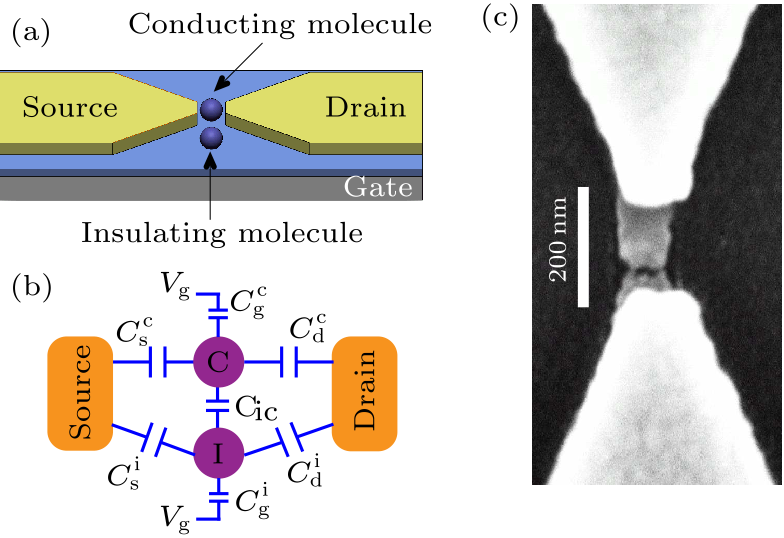
Fig. 1. (a) Schematic diagram of a single molecule device with an extra molecule aside. (b) Equivalent circuit diagram of the device in (a). (c) SEM image of the device after breaking.
The C$_{60}$ molecules are introduced before the current breaking process. Traditional molecule transfer methods are usually based on solution.[8,15] After preparing the chips containing gold nanowires or electrode pairs, researchers usually drop the solution of molecules onto the chips[17] or immerse the chips into the solution to absorb molecules.[19] However, continuously controlling the coverage of molecules is not easily carried out by the methods based on solution. What's more, organic dissolvent usually dissolves some contaminant from air or containers and may transfer the contaminant together with target molecules onto chips, which makes the devices' local environment more complicate. To well control the coverage and avoid the unexpected contaminant in solution, we use the thermal evaporation method to sublimate C$_{60}$ molecules onto the chips. During the molecule deposition process, the chips are placed in a high vacuum chamber and cooled by liquid nitrogen to make the molecules distribute uniformly on chips and to reduce the effect of thermal radiation. The C$_{60}$ molecules are evaporated from a K-cell evaporator with temperature 620 K. A shutter on the evaporator is used to control the deposition time precisely, which is essential to control the coverage of C$_{60}$ molecules on chips. After deposition of C$_{60}$ molecules, current breaking process is performed on nanowires to create electrode pairs. Then the chip is transferred to cryostat and cooled down to base temperature. The transport measurement was carried out at 1.4 K. A bias voltage $V_{\rm sd}$ was applied between source and drain electrodes and a gate voltage $V_{\rm g}$ was employed to tune the electron transport behavior. When the coverage of C$_{60}$ molecules on chip was low (less than 10% of all devices exhibiting different characteristics from a simple tunneling junction), all the devices would show similar transport behavior. The transport spectrum of a represent device is displayed in Fig. 2, in which differential conductance $dI/dV$ is plotted against $V_{\rm sd}$ and $V_{\rm g}$. In Fig. 2, two conductance peaks vary linearly with both $V_{\rm sd}$ and $V_{\rm g}$, forming a coulomb diamond pattern and revealing coulomb blockade behavior. From the measurement range, we can estimate the charging energy of the device shown in Fig. 2 exceeds 150 meV, consistent with the range of a single molecule and demonstrating that the features arise from a single C$_{60}$ molecule. Outside the blocking regions, there is also an excited conductance peak at 23 mV. The excited state at this energy scale is usually attributed to the vibronic states of the molecule devices.[20–22] When the electrons transport through the molecular devices, they could couple to the vibration degree of freedom of the molecules and thus form a conduction channel. Some states are internal from the molecule while some come from the interaction with electrodes.[15,23] The vibration states shown in different C$_{60}$ molecule devices are not identical because the local environments of molecules in different devices are not the same.
cpl-36-12-127301-fig2.png
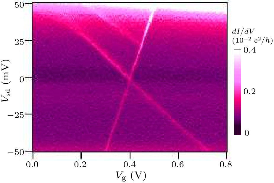
Fig. 2. Color plot of differential conductance ($dI/dV$) as functions of bias voltage ($V_{\rm sd})$ and gate voltage ($V_{\rm g})$ for a single C$_{60}$ molecule transistor. Here $e$ is the electron charge and $h$ is Planck's constant.
When we slightly increase the coverage of C$_{60}$ molecules on chips by extending the deposition time, most devices still show the regular coulomb blockade phenomenon similar to the device shown in Fig. 2. However, a few devices show a different behavior, and the transport spectrum from one of these devices is displayed in Fig. 3. The characteristic coulomb blockade pattern is still evident with an estimated charging energy more than 100 meV. There are also some excited levels with equal space in conducting regions, which is very similar to the previous study on single C$_{60}$ molecule transistors and may arise from the vibration of C$_{60}$ molecules on gold surface.[15] Outside the blocking region, the background differential conductance is strongly enhanced compared to the device in Fig. 2. This phenomenon may attribute to inelastic process induced by tunneling electrons and has been observed before in other single C$_{60}$ molecule transistor studies.[15] A striking feature in Fig. 3, which has not been observed in pure single C$_{60}$ molecule transistor, is the charge switching behavior. A pronounced charge offset can be observed between the left and right parts of the transport spectrum. The evolution of the switching forms a straight line with positive slope as functions of both gate and bias voltages. Charge switching behavior is observed quite frequently in single electron transistor devices, mainly caused by the charge traps on the surface of substrate, like defects. When a charge falls in (or leave) the trap, nearby single electron transistor devices will feel the electrostatic potential shift and the coulomb blockade condition would change accordingly. However, the switching behavior induced by surface charge traps does not depend on gate or bias voltage. It happens once and the transport changes permanently, causing a switching line parallel to the $V_{\rm sd}$ axis,[24] which is not our case. Considering our device fabrication process, the gate and bias dependent switching most likely comes from the influence of a nearby C$_{60}$ molecule.
cpl-36-12-127301-fig3.png
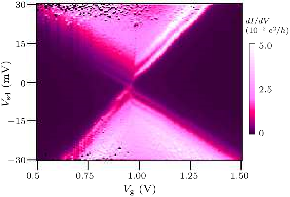
Fig. 3. Color plot of differential conductance ($dI/dV$) as functions of bias voltage ($V_{\rm sd})$ and gate voltage ($V_{\rm g})$ for a single C$_{60}$ molecule transistor with an extra molecule aside.
To confirm our assumption, we utilize a quantum dot model to examine the unique transport behavior. When an extra side molecule residing very close to a single molecule transistor device forming the structure shown in Fig. 1(a), two molecules together with electrodes form a parallel double quantum dot system[25] and the equivalent circuit is displayed in Fig. 1(b). We label the side molecule as insulating molecule(I) and device's molecule as conducting molecule(C). The conducting molecule shows tunneling coupling to both source and drain electrodes, so electrons can transport through conducting molecule forming the coulomb blockade pattern in Fig. 3. For the insulating molecule, the tunneling rate from molecule to one or both of the electrodes is too low to be measureable. The chemical potential of insulating molecule can still be tuned by bias or gate voltage like the conducting molecule. Particularly, there is also capacity coupling between two molecules, namely the chemical potentials of two molecules can be affected by each other. Then the charge switching pattern in Fig. 3 can be explained by the charge state variation of the insulating molecule. When one electron enters into or leaves from the insulating molecule, the conducting molecule will experience an additional potential, which shifts its coulomb pattern. The switching line in Fig. 3 corresponds to the situation when an electron tunnels on or off the insulating molecule. There are two possible paths for an electron tunnels on(off) the insulating molecule. One path is that the electron is transferred between insulating molecule and one electrode (source or drain, not both). In this situation, higher gate voltage will stabilize the insulating molecule with one more electrons, which provides an extra negative potential on the conducting molecule, leading its coulomb pattern shift right along the $V_{\rm g}$ axis. This is opposite to what we observe in Fig. 3, in which the pattern shifts left, indicating one less electron for the insulating molecule at higher gate voltage. Another way is that the electron is transferred between the insulating molecule and conducting molecules, namely a tunneling coupling existing between two molecules. In this situation, the electron exchange between the insulating molecule and any electrodes must be impossible, otherwise there will be addiction conductance peak appearing in Fig. 3, as additional pathway for electron transport is formed.[26] In this case, the insulating molecule can be stabilized with one less electron at higher gate voltage if its chemical potential is higher than the conducting molecule, when the electron tunnels from the insulating molecule to the conducting molecule. The switching line apparently indicates the situation that the two molecules exchange electrons, namely the chemical potentials of the two molecules are equal. Based on the above analysis, we can discuss the switching behavior quantitatively using the double-quantum-dot model shown in Fig. 1(b). Denote the chemical potential of two molecules as $\mu ^{\rm c}$ and $\mu ^{\rm i}$ (c stands for conducting molecule and i for insulating molecule). The switching line follows the relation $\mu ^{\rm c}=\mu ^{\rm i}$. We simplify the analytic process by assuming $C_{\mathrm{ic}}\ll C_{s}^{\rm c}, C_{d}^{\rm c}, C_{\rm g}^{\rm c}, C^{\rm c}$, where $C^{\rm c}$ is the total capacity of the conducting molecule and $C^{\rm c}=C_{s}^{\rm c}+C_{d}^{\rm c}+C_{\rm g}^{\rm c}$. Then the chemical potential of the conducting molecule, $\mu ^{\rm c}$, is given by $$ \mu ^{\rm c}=\mu _{0}^{\rm c}-\vert e\vert \left(V_{\mathrm{sd}}\frac{C_{s}^{\rm c}}{C^{\rm c}}+V_{\rm g}\frac{C_{\rm g}^{\rm c}}{C^{\rm c}}\right),~~ \tag {1} $$ where $\mu _{0}^{\rm c}$ is the chemical potential of the conducting molecule when $V_{\rm sd}$ and $V_{\rm g}$ are zero. As the electrons cannot be transferred between the insulating molecule and source/drain electrodes, the location of the insulating molecule must be outside the tunneling range of both source and drain electrodes. The electron exchange is possible between the insulating and conducting molecules, indicating that the distance between the insulating molecule and source/drain electrodes is larger than the distance between the two molecules. Thus the capacity of the insulting molecule to electrodes tends to be smaller than the intermolecular capacity, i.e. $C_{s}^{\rm i}, C_{d}^{\rm i} < C_{\mathrm{ic}}$. Then the influence on the insulating molecule from potential variation of electrodes is weak compared to the potential change of the conducting molecule. In order to simplify the analytic process, we use zero-order approximation and neglect the influence from the electrodes, namely assuming $C^{\rm i}\approx C_{\mathrm{ic}}+C_{\rm g}^{\rm i}$, where $C^{\rm i}$ is the total capacity of the insulating molecule. As will be shown later, this approximation does not affect the result significantly. Then the chemical potential of the insulating molecule can be expressed as $$ \mu ^{\rm i}=\mu _{0}^{\rm i}-\frac{C_{\mathrm{ic}}}{C^{\rm i}}\left( \mu ^{\rm c}-\mu _{0}^{\rm c} \right)-\vert e\vert V_{\rm g}\frac{C_{\rm g}^{\rm i}}{C^{\rm i}},~~ \tag {2} $$ where $\mu _{0}^{\rm i}$ is also a constant. Based on formulae (1) and (2), the slope of the charge switching line can be deduced using $\mu ^{\rm c}=\mu ^{\rm i}$ and expressed as $$ k=1+C_{d}^{\rm c}/C_{s}^{\rm c},~~ \tag {3} $$ in which $C_{d}^{\rm c}/C_{s}^{\rm c}$ can be obtained by the slope of the coulomb pattern edge in Fig. 3 and equals 0.54. Thus the calculating slope of charge switching line is 1.54, very close to the measurement result $k=1.30$ in Fig. 3, strongly proving that our assumption and model analysis are reasonable. As shown in formula (3), the slope of charge switching line depends only on the configuration of the conducting molecule. The slope is always positive and greater than 1. The reason for lacking of negative slope is that the bias is only applied on the source electrode but not symmetrically on both source and drain electrodes. We calculate the ground state transport spectrum using the model in Fig. 1(b) by the rate equation approach,[27] based on formulae (1) and (2). The calculation result is shown in Fig. 4, clearly reproducing the charge switching feature in Fig. 3. It is worth noting that the above configuration is deduced totally by analyzing the transport result. We are not able to confirm this configuration further by other experimental methods as it is technically impossible to image a single molecule device directly now. However, we can still argue that this influence is from a nearby molecule but not other kinds of nanoparticles. The charging energy of general nanoparticles is much smaller than a single molecule, making it possible to charge the particle several times within the voltage range of our measurement. As a result, many parallel charge switching lines will appear, like the result shown in double P dopants quantum dots on silicon surface.[28] We only observe a single switching line in our devices, proving that the influence is from another single C$_{60}$ molecule.
cpl-36-12-127301-fig4.png
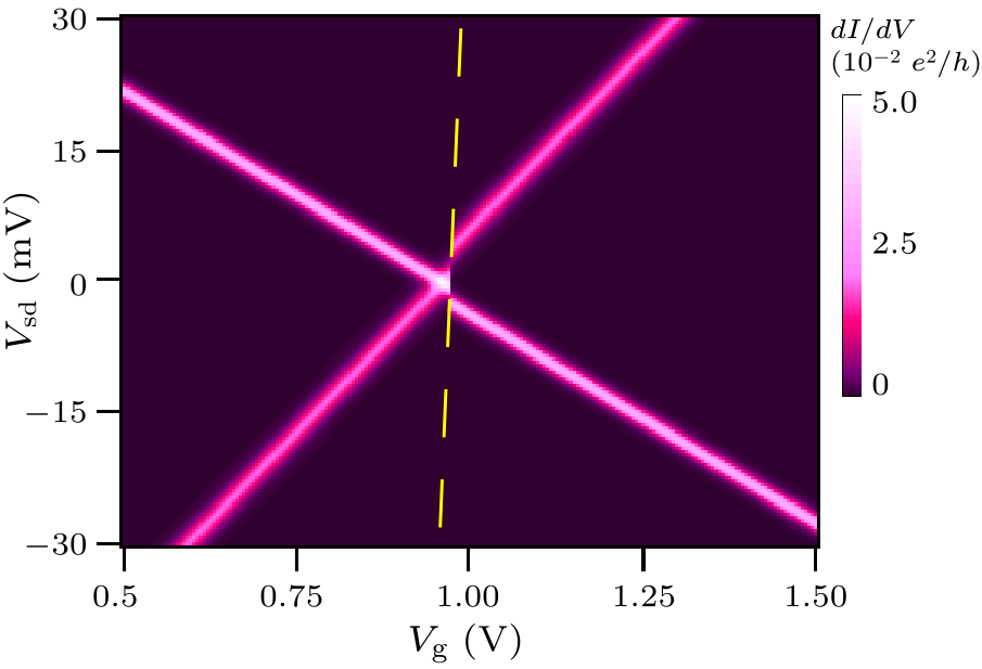
Fig. 4. Two-dimensional differential conductance map calculated by rate equation using the model in Fig. 1(b). The charge switching boundary is marked by the yellow dashed line.
cpl-36-12-127301-fig5.png
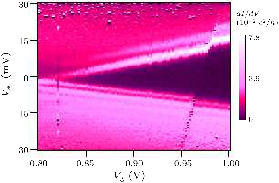
Fig. 5. Two-dimensional differential conductance map for the same device of Fig. 3 after thermal stimulate.
We also experimentally investigated the effect of local charging environment variation on the intermolecular interaction by treating the devices with thermal stimulation. For single-molecule devices, the local charging environment would alter at different cooldowns, appearing as a shift of the coulomb pattern. We heated the devices from 1.4 K to 4.2 K and held it there for several hours. Then the devices were cooled down to base temperature again. Figure 5 shows the transport spectrum from the same device of Fig. 3 after thermal treatment. The general coulomb pattern with charge switching is still pronounced, revealing that the interaction between the two molecules is preserved to be of capacity and tunneling. The whole coulomb pattern shifts left but keeps the slope of the edges unchanged. The slope of charge switching line in Fig. 4 is also identical to that in Fig. 3, which confirms the relation in formula (3) again. In conclusion, we have studied the transport behavior of a single C$_{60}$ molecule transistor when another C$_{60}$ molecule in vicinity. It is found that the charging of the nearby molecule strongly affects the transport behavior of a single molecule device, leading to a decisive change in its transport spectrum from a pure single molecule transistor device. These features are caused by capacity and tunneling coupling from nearby molecules. When the charge state of the nearby molecule is modified, an additional potential is applied to the single molecule device, leading its chemical potential to shift a certain amount. The charge switching line with positive slope is determined by the situation when two molecule exchanging electrons. These results illustrate how a single molecule affects the transport behavior of a nearby molecular device, and gain deeper understanding on the interaction between two molecules down to single molecule scale.
References Single-molecule junctions beyond electronic transportSingle Molecule Electronic DevicesElectron transport in molecular junctionsMolecular-Scale Electronics: From Concept to FunctionSingle-molecule transistorsKondo Resonances in Molecular DevicesSingle-molecule transport in three-terminal devicesKondo resonance in a single-molecule transistorSingle-electron transistor of a single organic molecule with access to several redox statesElectroluminescence from a single nanotube–molecule–nanotube junctionElectrostatic control of thermoelectricity in molecular junctionsElectrically driven nuclear spin resonance in single-molecule magnetsGating a single-molecule transistor with individual atomsMolecular junctions based on aromatic couplingNanomechanical oscillations in a single-C60 transistorThe Kondo Effect in C 60 Single-Molecule TransistorsSuperconductivity in a single-C60 transistorFabrication of metallic electrodes with nanometer separation by electromigrationRoom-Temperature Gating of Molecular Junctions Using Few-Layer Graphene Nanogap ElectrodesInelastic Electron Tunneling via Molecular Vibrations in Single-Molecule TransistorsMolecular transport junctions: vibrational effectsAddition Energies and Vibrational Fine Structure Measured in Electromigrated Single-Molecule Junctions Based on an Oligophenylenevinylene DerivativeVibrational Excitation in Single-Molecule Transistors: Deviation from the Simple Franck−Condon PredictionUniversality of the two-stage Kondo effect in carbon nanotube quantum dotsSingle electron switching in a parallel quantum dotFull characterization of a carbon nanotube parallel double quantum dotTheory of Coulomb-blockade oscillations in the conductance of a quantum dotCharge Sensing of Precisely Positioned P Donors in Si
[1] Aradhya S V and Venkataraman L 2013 Nat. Nanotechnol. 8 399
[2] Song H, Reed M A and Lee T 2011 Adv. Mater. 23 1583
[3] Tao N J 2006 Nat. Nanotechnol. 1 173
[4] Xiang D et al 2016 Chem. Rev. 116 4318
[5] Perrin M L, Burzuri E and van der Zant H S 2015 Chem. Soc. Rev. 44 902
[6] Scott G D and Natelson D 2010 ACS Nano 4 3560
[7] Osorio E A et al 2008 J. Physics. Condens. Matter: An Inst. Phys. J. 20 374121
[8] Liang W J et al 2002 Nature 417 725
[9] Kubatkin S et al 2003 Nature 425 698
[10] Marquardt C W et al 2010 Nat. Nanotechnol. 5 863
[11] Kim Y et al 2014 Nat. Nanotechnol. 9 881
[12] Thiele S Thiele et al 2014 Science 344 1135
[13] Martínez-Blanco J et al 2015 Nat. Phys. 11 640
[14] Wu S et al 2008 Nat. Nanotechnol. 3 569
[15] Park H et al 2000 Nature 407 57
[16] Yu L H and Natelson D 2004 Nano Lett. 4 79
[17] Winkelmann C B et al 2009 Nat. Phys. 5 876
[18] Park H et al 1999 Appl. Phys. Lett. 75 301
[19] Prins F et al 2011 Nano Lett. 11 4607
[20] Yu L H et al 2004 Phys. Rev. Lett. 93 266802
[21] Galperin M, Ratner M A and Nitzan A 2007 J. Phys.: Condens. Matter 19 103201
[22] Osorio E A et al 2007 Adv. Mater. 19 281
[23] de Leon N P et al 2008 Nano Lett. 8 2963
[24] Petit P et al 2014 Phys. Rev. B 89 115432
[25] Hofmann F et al 1995 Phys. Rev. B 51 13872
[26] Abulizi G, Baumgartner A and Schönenberger C 2016 Phys. Status Solidi B 253 2428
[27] Beenakker C W J 1991 Phys. Rev. B 44 1646
[28] Mahapatra S, Buch H and Simmons M Y 2011 Nano Lett. 11 4376