Chinese Physics Letters, 2021, Vol. 38, No. 7, Article code 074201 Polarity Reversal of Terahertz Electric Field from Heavily p-Doped Silicon Surfaces Hai-Zhong Wu (吴海忠)1†, Quan Guo (郭泉)2†, Yan-Yun Tu (涂艳云)1, Zhi-Hui Lyu (吕治辉)1, Xiao-Wei Wang (王小伟)1, Yong-Qiang Li (李永强)1, Zhao-Yan Zhou (周兆妍)1, Dong-Wen Zhang (张栋文)1*, Zeng-Xiu Zhao (赵增秀)1, and Jian-Min Yuan (袁建民)1,3* Affiliations 1College of Liberal Arts and Sciences, National University of Defense Technology, Changsha 410073, China 2Northwest Institute of Nuclear Technology, Xi'an 710024, China 3Graduate School of China Academic of Engineering Physics, Beijing 100193, China Received 1 April 2021; accepted 28 April 2021; published online 3 July 2021 Supported by the National Key Research and Development Program of China (Grant No. 2019YFA0307704), the NSAF Joint Fund (Grant No. U1830206), the Major Research Project of National Natural Science Foundation of China (Grant No. 91850201), and the National Natural Science Foundation of China (Grant Nos. 11974426, 11974425, 11874425, 11774428, and 12074431).
They contributed equally to this work.
*Corresponding authors. Email: dwzhang@nudt.edu.cn; jmyuan@gscaep.ac.cn
Citation Text: Wu H Z, Guo Q, Tu Y Y, Lyu Z H, and Wang X W et al. 2021 Chin. Phys. Lett. 38 074201    Abstract Above-band-gap optical excitation of electron-hole pairs screens the doping-induced surface electric field and generates terahertz (THz) pulses via free-carrier transport. THz emission from a heavily doped silicon surface is much weaker than that of lightly doped samples. A polarity reversal of the THz electric field is observed in heavily doped p-type silicon, indicating that the doping related and carrier induced surface electric fields oppose each other. By comparing the penetration depth of the excitation laser with the thickness of the depletion layer for the doped silicon, it is shown that competition between diffusion and drift current causes the polarity reversal. DOI:10.1088/0256-307X/38/7/074201 © 2021 Chinese Physics Society Article Text As device dimensions continue to shrink, surface becomes more important and surface-to-volume ratios increase. Dopant density and distribution in semiconductors strongly affect the surface states and hence the device performance.[1] The silicon surface has traditionally been a major topic in fabrication of electronic devices. It also underpins numerous modern technologies ranging from complementary metal oxide semiconductor (CMOS) to novel concepts in light-emitting diodes and solar cells.[2–5] Silicon device fabrication is facilitated with a nondestructive, noncontact in situ probe of doping. However, the current means of doping characterization feature certain drawbacks in terms of limited precision, ambiguity of measurement interpretation, or limited applicability under realistic device conditions. Electric methods require considerable surface area for contact, which dramatically changes the surface states on the interface. These constraints preclude the measurements under typical device working conditions.[6] Optical probes such as the optical second-harmonic generation (SHG) are versatile but has long been difficult to resolve the dopant type.[7–10] The time-dependent second-harmonic generation (TD-SHG) measurement indicated that the doping-related and carrier transportation induced interfacial electric fields oppose each other in heavily doped p-type samples.[11,12] However, recent experiment showed similar SHG signals for both lightly and heavily p-doped Si surfaces after long radiation time.[13] THz emission from semiconductor surface is influenced by the sign and strength of the interfacial electric field as well as the relaxation dynamics of the photoinduced carriers.[14–16] Currently, there is a considerable interest in exploring THz electric-field transient as a powerful, noncontact method of studying hot carrier dynamics[17,18] and material properties of semiconductors.[17–26] At bare semiconductor surfaces, band-bending and a surface-space-charge region exists due to the pinning of the Fermi level at the energetic position of charged surface states.[27] The strength and sign of the build-in static electric field are sensitive to the dopant concentration and type as well as the thickness of the depletion layer. After optical excitation, electron-hole separation due to the internal electric-field rapidly screens the surface field. This fast depolarization of the initial surface field forms the drift current and emits THz radiation. The change of the direction of the drift current is revealed as a polarity reversal of the generated THz transient going from p- to n-type semiconductor as observed in GaAs.[28,29] Concurrently, an electronic dipole and the subsequent diffusion current is built up because the electron population diffuses more rapidly than the hole population. The photo-Dember field points to the surface and the consequential THz emission is independent of the dopant type.[30,31] THz electric-field transient can be a noninvasive, in situ probe of the interfacial field consisting of quiescent and dynamics components. The screening dynamics of the initial surface field depends on the competition between optically injected carrier density and the doping density.[27] At the fixed excitation optical flux, the complete screening occurs already during the excitation pulse in the lightly doped samples and the diffusion current plays a leading role in THz emission. While in the heavily doped samples, only partial screening occurs, and the drift current emerges corresponding to THz radiation. Our recent discovery on the polarity reversal of the THz waveform from a heavily doped p-type silicon (001) surface provided the motivation to inquire whether THz electric-field transient would be sensitive to dopant concentration and type.[13] In this Letter, we therefore investigate systematically THz emission from (001) and (111) silicon surface with different doping types and densities. It is found that the doping-related and carrier induced interfacial electric fields oppose each other in heavily doped p-type silicon surfaces. As the dopant increases for lightly doped silicon, the amplitude of THz electric-field increases for n-doped silicon, while decreases for p-doped silicon. These observations indicate that THz emission is a sensitive, noncontact probe of dopant type and concentration at silicon surfaces. All samples investigated here were doped silicon wafers of (001) and (111) surface orientation (Kejing, Hefei, China) with doping concentrations (resistivities) between $ < 6 \times 10^{12}$ cm$^{-3}$ ($> 2000\,\Omega$$\cdot$cm) and $> 8.5 \times 10^{18}$ cm$^{-3}$ ($ < 0.01\,\Omega$$\cdot$cm). All wafers were 500 µm thick and prepared according to the process in Ref. [13]. The carrier densities were measured using THz time-domain transmission spectroscopy and THz time-domain reflection spectroscopy. All samples were exposed to ambient air for sufficient time to form a native oxide layer with a thickness of approximately 3 nm that covered the entire sample surface. Before the measurements, the sample surfaces were cleaned using successive sonication processes in acetone and deionized water. As stated by Park and his coworkers, no significant differences between the as-received native oxide interface and the regrown native oxide interface were observed in the time-dependent SHG measurements, indicating that the as-received native oxide interface and the regrown native oxide interface have similar interface properties.[32] To investigate THz emission as a potential probe of semiconductor doping, THz time-domain spectroscopy (THz-TDS) experiments were performed on Si surfaces using a laser system providing p-polarized light pulses centered at a wavelength of 800 nm with 150 fs duration and 76 MHz repetition rate, as described in detail earlier.[13] A maximum laser pulse energy of 10 nJ was accessible and the peak intensity of the focused pump beam was approximately 1.5 GW/cm$^2$. The sample could be rotated about the surface normal to measure the azimuthal dependence. In the reflection, the terahertz emission and SHG from sample surfaces were detected with different systems, respectively. A 3-mm-thick ZnTe (110) wafer was used to detect terahertz electric-field transient. The intensity of SHG at $\lambda =400$ nm was detected by a photo-multiplier tube. All the measurements were performed in air at room temperature. It took about 2 min to record the THz waveform by using the step-scanned time-delay line. For virgin “cold” samples, the SH signal increased steadily on the time scale of minutes and saturated, which consistently reproduced the result reported in TD-SHG experiment for “lightly doped” Si samples.[11] We recorded the experimental data after 10 min of laser pumping on samples. The photoexcited “hot” samples reached their quasi-equilibrium values by screening the surface-space-charge field. The setup used a lock-in amplifier in combination with a 1200 Hz light chopper to the SH and THz signals, which monitored the second time derivative of the polarization at the Si surfaces.
cpl-38-7-074201-fig1.png
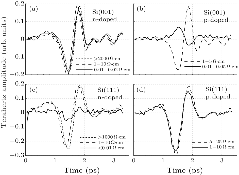
Fig. 1. Terahertz electric-field transients from (a) n-, (b) p-type Si (001) and (c) n-, (d) p-type Si (111) surfaces with different doping concentrations.
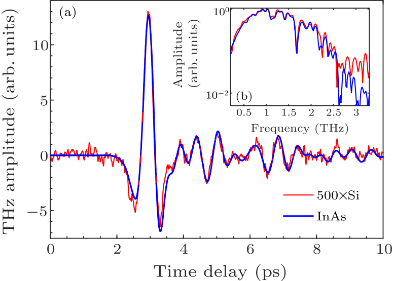
Figure 1 shows the terahertz waveforms radiated from Si (001) and (111) surfaces with different doping types and concentrations. All curves are recorded after irradiation times of 600 s to stabilize the SH and THz signals. As shown in Fig. 1, THz waveforms are similar for lightly doped Si surfaces independent of the doping type, and THz emission decreases dramatically with dopant density above $10^{18}$ cm$^{-3}$ ($ < 0.01\,\Omega$$\cdot$cm) for both n- and p-type Si. This trend supports the result that the initial SHG intensities are similar and increase with dopant density only above $10^{17}$ cm$^{-3}$.[12] Interestingly, the THz waveform flips only in the heavily doped p-type sample with doping density of 0.75–$8.5 \times 10^{18}$ cm$^{-3}$ (0.01–0.05 $\Omega$$\cdot$cm). As can be seen in Fig. 1, all of the lightly doped samples (doping density $ < 10^{18}$ cm$^{-3}$) show similar THz waveforms regardless of the dopant type. This behavior has been observed from InAs that is known to be a strong photo-Dember emitter under the excitation of 800 nm.[30,31] We therefore compared the THz waveforms emitted from lightly n-doped Si (111) (1–10 $\Omega$$\cdot$cm) and the p-InAs wafer. As shown in Fig. 2, the waveform from lightly doped Si exactly agrees with that from p-InAs if the THz electric field from Si surface is magnified 500 times. This result reveals that THz emission from lightly doped Si samples is dominated by a very weak contribution from the diffusion of electrons and holes after the photoexcitation.[33,34] Silicon wafers with a resistivity higher than 1 $\Omega$$\cdot$cm (doping concentration $ < 1.2 \times 10^{16}$ cm$^{-3}$) show a similar behavior as presented in Fig. 1.
cpl-38-7-074201-fig2.png
Fig. 2. THz electric-field transients (a) and normalized amplitudes (b) from lightly doped n-type Si (111) surface (red line) and p-type InAs wafer (blue line).
cpl-38-7-074201-fig3.png
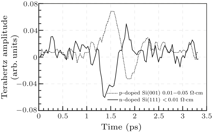
Fig. 3. THz electric-field transients from heavily doped p- (dotted line) and n-type (solid line) Si surfaces.
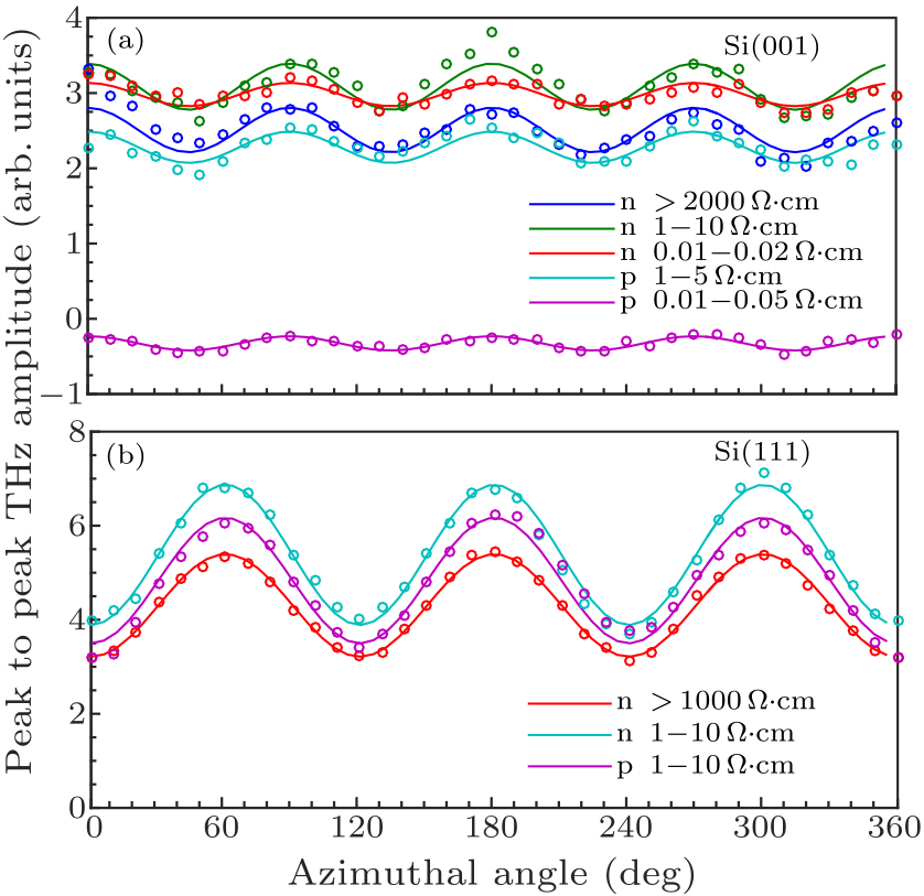
Figure 3 shows the THz waveform from heavily doped Si surfaces. THz radiation is much weaker compared with the lightly doped Si surfaces. The reversed polarity going from n- to p-type doping, reminiscent of the drift current in the well-known GaAs.[27,29] These results underline the strong doping dependence of the surface field and support the results on surface-electric-field induced SHG at Si/SiO$_{2}$ interfaces.[11,12] Figure 4 shows the terahertz emission from Si surfaces with different doping densities for Si (001) and Si (111) surface orientation. The samples are excited by the femtosecond laser with photon energy of 1.55 eV at an incident angle of 45$^{\circ}$. Both the pump laser and the detected THz radiation are p-polarized. The azimuth $\varphi$ was the angle between the incidence plane and [100] direction for Si (001) or the $[21\overline 1 ]$ direction for Si (111). The p-polarized THz emission reveals cos(4$\varphi$) and cos(3$\varphi$) modulation for Si (001) and Si (111) wafers, respectively. The hollow circles are the experimental data, and the solid curves are the fitting results. The peak-to-peak THz electric field shows obvious anisotropy for both oriented Si wafers in addition to the azimuthally independent contribution from the diffusion and drift current as demonstrated in our previous work.[13] The azimuthal dependent component of THz emission originates from the nonlinear polarization due to the bulk electric quadrupole and magnetic dipole polarization, which is determined by the superposition of initial surface space-charge and carrier induced field and not the concern of the current work.[13] Figure 4(a) shows the THz emission from the Si (001) surfaces. Under similar doping concentrations, the n-doped sample (1–10 $\Omega$$\cdot$cm) radiated THz waves stronger than the p-doped sample (1–5 $\Omega$$\cdot$cm). For the n-doped samples, THz emission enhanced when the doping density increased from $10^{12}$ cm$^{-3}$ ($> 2000\,\Omega$$\cdot$cm) to $10^{15}$ cm$^{-3}$ (1–10 $\Omega$$\cdot$cm) or $10^{18}$ cm$^{-3}$ (0.01–0.02 $\Omega$$\cdot$cm). However, for p-doped samples, THz emission decreases with increasing doping concentration while the SH signals are almost the same as in our early work.[13] The dramatically reduced THz radiation appears as the reversed polarity in the heavily p-doped sample (0.01–0.05 $\Omega$$\cdot$cm). Figure 4(b) supports the same trends for Si (111) surfaces. For the samples with similar doping density, the n-type sample (1–10 $\Omega$$\cdot$cm) emits THz more efficiently than the p-type sample (1–10 $\Omega$$\cdot$cm). For n-doped samples, the sample (1–10 $\Omega$$\cdot$cm) with a higher doping concentration is a better THz emitter compared to the lightly doped sample ($> 1000\,\Omega$$\cdot$cm).
cpl-38-7-074201-fig4.png
Fig. 4. Peak-to-peak amplitudes of THz electric fields as a function of the azimuthal angle of (a) Si (001) and (b) Si (111) surfaces.
At flat band voltages in both n- and p-silicon MOSs, THz emission from the diffusion current depends on the effective mass and shows the anisotropy.[16,20,22] Figure 4(b) shows that the THz electric field from a lightly doped Si (111) surface is 1.8 times stronger than that from Si (001), which agrees with the ratio of diffusion coefficient of electrons after the photoexcitation. The effective electron mass $m^*$ in Si crystal is $0.916 m_{0}$ and $0.258 m_{0}$ along the (001) and (111) orientations, respectively.[35] Here $m_{0}$ is the mass of free electron. The diffusion coefficient of photoelectrons is inversely proportional to the square root of $m^*$. This result as well as doping dependence supports that THz emission from lightly doped Si (111) surfaces is dominated by the very weak contribution from the diffusion current.
cpl-38-7-074201-fig5.png
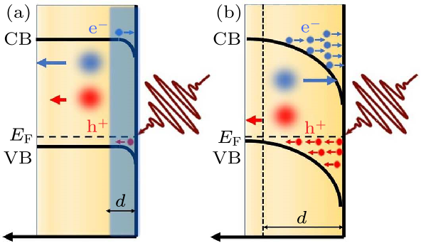
Fig. 5. Optical excitation of hot carriers in lightly (a) and heavily (b) p-doped Si. Photogenerated hot electron-hole (e–h) pairs (blue and red circles, respectively) are separated to a distance $d$ forming a dipole to screen the initial quiescent electronic field at the p-doped Si surfaces. The screen length is thin in (a) shown as the blue region and thick in (b) depicted as the dashed line. The energies of conduction band (CB, horizontal solid line), valence band (VB, horizontal solid line) and Fermi level (EF, horizontal dashed line) are shown. The incident photo (brown arrow) energy is higher than the direct bandgap ($E_{\rm g}$) of Si.
Silicon is a semiconductor with a rather low electron mobility. If the sample is moderately doped, the Fermi level is close to the mid-band gap, where the density of surface states is relatively small. Thereby, in moderately doped samples, the charge density accumulated in the interface and the static electric field are smaller than those in heavily doped samples as shown in Fig. 5(a). In the heavily p-doped Si, the Fermi level lies close to the silicon valence band edge. Hence the downwards band-bending in the order of 0.5 eV occurs near the surface and the resultant internal electric field in the order of $\ge$$10^{4}$–$10^{5}$ V/cm points towards the bulk[11] as shown in Fig. 5(b). In the heavily n-doped Si, the Fermi level lies close to the silicon conduction band edge and the internal electric field points into the surface. When photons of the energy 1.55 eV irradiate the Si surface, the electron-hole pairs are generated by one-photon absorption via the indirect optical transition. Single-photon absorption in silicon needs electron-phonon coupling. Therefore, the lifetime of electron-hole pairs for one-photon absorption is long to about 1 µs.[36] In our THz-TDS experiment, all the samples were excited for 10 min by 800 nm femtosecond pulses to reach their quasi-equilibrium values by screening the surface space charge. Single laser pulses induced the deviation of the surface-polarization from the quiescent state and recorded in the experiment. Above-band-gap optical excitation of electron-hole pairs within the surface-space-charge region screens the doping-induced interfacial electric field via free-carrier transport. The superposition field of quiescent doping charge and dynamically photoinjected carriers determines the direction and amount of band bending as well as THz emission. The screening dynamics for both types of doping are dominated by majority carriers, which are driven into the bulk, thus building up effective polarization to cancel the initial space-charge field. This polarization reduces the thickness of the initial depletion layer and flattens the surface band due to further redistribution of the charge carriers.[29] We can understand the screen dynamics in silicon with different doping densities in the following intuitive way. The initial surface field is screened by the polarization which is built up from electron-hole separation, i.e., $$ \Delta P(t)=qN_{\rm eh} (t,z)d(t), $$ where $d(t)$ is the spatial separation of photoinjected electrons and holes, $\Delta P(t)$ is the associated polarization, and $N_{\rm eh} (t,z)$ is the carrier density generated by the photoexcitation. The screening degree depends on the difference between the optically injected carrier density and the doping density. The screen length $d(t)$ is proportional to the doping charge density according to the above equation. In the lightly doped Si samples as shown in Fig. 5(a), the charge density accumulated in the interface is small and can be screened completely by the photogenerated e–h densities with a short distance under the experimental photon flux. The absorption coefficient of lightly doped Si on 1.55 eV photons is small and the penetration depth is much longer[37] than carrier separation $d(t)$.[13,38] Most carriers are photogenerated in a region of negligible electric field to form a diffusion current, which is independent of the doping type as observed in InAs.[30,31] While for the heavily doped Si samples, the density of the surface charge trapped at the surface states is high and can only be partially screened by the photoinjected carriers under the experimental photon flux. The carrier separation distance $d(t)$ is comparable with the penetration depth in heavily doped Si wafers as shown in Fig. 5(b). Most photoinjected carriers experience the space-charge field to form a drift current, of which the direction depends on the doping type as observed in GaAs.[28,29] After 10 min of radiation, the electrons are steadily injected to the surface. In our experiment, the peak laser intensity is 1.5 GW/cm$^{2}$ and the photogenerated e–h densities $N_{\rm eh}$ is about $2.4 \times 10^{17}$ cm$^{-3}$. For p-type Si, the charge carried by the photoinjected electrons cancels the initial interface positive charge and additional photoinjected electrons and holes diffuse into the bulk. This indicates that the doping related initial space-charge-field and the diffusion-induced field of photoinjected carriers oppose each other in p-doped Si surfaces. When the resistivity of the p-doped Si is higher than 1 $\Omega$$\cdot$cm (doping density $ < 1.2 \times 10^{16}$ cm$^{-3}$), the initial doping related field is completely screened by the photoinjected carriers. The magnitude of the diffusion current beneath the surface decreases with the increase of p-type doping density because more photon-injected electrons are attracted to the initial positive charge at the interface to neutralize the space-charge field while holes are swept away from the interface. Thus, the far-field THz emission is weaker with the increase of the p-type doping concentration. While for n-type Si, screening electrons are swept toward the bulk by the initial doping field, enhancing the diffusion current as well as THz emission. Therefore, THz emission from n-doping samples is slightly stronger than that from the p-type samples with a similar concentration as shown in Fig. 4. The THz electric field is slightly larger, increasing the doping concentration for n-type samples. THz intensity can be used to probe the built-in electric field as well as the doping type and concentration. For heavily doped Si, photoinjected carriers only partially screen the initial surface-space-charge and are drifted by the residual surface-space field. The doping concentration is $> 8.5 \times 10^{18}$ cm$^{-3}$ for n-type Si (111) and $7.5 \times 10^{17}$–$8.5 \times 10^{18}$ cm$^{-3}$ for p-type Si (001), respectively, which are both higher than the photoinjected carrier density $2.4 \times 10^{17}$ cm$^{-3}$. As shown in Fig. 3, the THz emission is dramatically reduced for heavily doped samples, to which the unscreened weak surface-charge fields contributed. The flipped THz waveform shows that the initial doping and the carrier induced electric fields oppose each other. Previous time-resolved SHG experiments indicated that initial SH signals are independent of the dopant type and only increase significantly with the dopant concentration over $10^{18}$ cm$^{-3}$ with the peak pumping intensity of 1.3 GW/cm$^2$.[11] Our earlier experiment also showed that SH signals from the p-type Si (001) surface with dopant concentration of $7.5 \times 10^{17}$–$8.5 \times 10^{18}$ cm$^{-3}$ maintain the same as the lightly p-doped sample with the density of $2.8 \times 10^{15}$–$1.3 \times 10^{16}$ cm$^{-3}$ pumped with 1.5 GW/cm$^2$.[13] For a wide range of dopant concentrations, the SHG probe depth is smaller than the extent of the space-charge region $d(t)$ shown in Fig. 5 and insensitive to the dopant type and concentration.[12] On the contrary, THz electric-field transient is sensitive to the dynamics of photoinjected carriers driven by the residual surface-space field extending to a large distance $d(t)$ as in Fig. 5(b), which can be used to probe the dopant type (polarity reversal) and concentration (change of amplitude). In conclusion, doping and photon-excitation determines the transport dynamics of optically generated free electron-hole pairs and the associated screening of the internal electric field beneath the Si surfaces as well as THz transient. Drift current dominates THz emission in heavily doped Si surfaces under the excitation with low photon flux. While diffusion current leads to THz transient in lightly doped Si surface because of the fast and complete screening of the surface charge by the high concentration of photoinjected carriers. THz emission measurements applying femtosecond laser pulses to heavily doped Si surface reveal a dramatically reduced amplitude of the THz electric field in comparison with that of lightly doped samples. A polarity reversal of the THz electric field is observed in the heavily doped p-type Si surface relative to that of heavily doped n-type sample. For lightly doped ($ < 10^{18}$ cm$^{-3}$) Si surfaces, THz electric-field transient assumes a similar waveform while the amplitude is affected by the surface-charge field. As the doping increases, the amplitude of THz electric field increases for n-type Si, and decreases for p-type Si. These results indicate that THz emission is a sensitive, noncontact probe of dopant type and concentration at Si surface, which may facilitate the fabrication and processing of shallow silicon-based junctions and metamaterials employing ultrathin oxide layers.
References Point defects and dopant diffusion in siliconCoupled Electron-Hole Dynamics at the Si / SiO 2 InterfaceElectron Photoinjection from Silicon to Ultrathin Si O 2 Films via Ambient OxygenElectronic Transitions at Si(111)/Si O 2 and Si(111)/S i 3 N 4 Interfaces Studied by Optical Second-Harmonic SpectroscopyBand structure evolution during the ultrafast ferromagnetic-paramagnetic phase transition in cobaltOptical Second Harmonic Spectroscopy of Boron-Reconstructed Si(001)Multiphoton photoemission and electric-field-induced optical second-harmonic generation as probes of charge transfer across the S i / S i O 2 interfaceSurface-step-terrace tuned second-order nonlinear optical coefficients of epitaxial ferroelectric BaTiO 3 filmsCharacterization of domain distributions by second harmonic generation in ferroelectricsIonization and shielding of interface states in native p+-Si/SiO2 probed by electric field induced second harmonic generationSecond harmonic generation probing of dopant type and density at the Si/SiO2 interfaceTerahertz emission and optical second harmonic generation from Si surfacesGeneration of femtosecond electromagnetic pulses from semiconductor surfacesOptoelectronic measurement of semiconductor surfaces and interfaces with femtosecond opticsSimplified formulas for the generation of terahertz waves from semiconductor surfaces excited with a femtosecond laserCarrier dynamics in semiconductors studied with time-resolved terahertz spectroscopyUltrafast spatiotemporal photocarrier dynamics near GaN surfaces studied by terahertz emission spectroscopyMaterials for terahertz science and technologyProbing the surface potential of oxidized silicon by assessing terahertz emissionSurface Optical Rectification from Layered MoS 2 Crystal by THz Time-Domain Surface Emission SpectroscopyNoncontact evaluation of electrical passivation of oxidized silicon using laser terahertz emission microscope and corona chargingCharacterization of through-silicon vias using laser terahertz emission microscopyControl of dipole properties in high-k and SiO 2 stacks on Si substrates with tricolor superstructureTerahertz Emission Spectroscopy and Microscopy on Ultrawide Bandgap Semiconductor β-Ga2O3THz Time-Domain Spectroscopic Ellipsometry With Simultaneous Measurements of Orthogonal PolarizationsSubpicosecond carrier transport in GaAs surface-space-charge fieldsSimulation of terahertz generation at semiconductor surfacesDiffusion and drift in terahertz emission at GaAs surfacesTerahertz radiation from InAs induced by carrier diffusion and driftTerahertz emission from (100) InAs surfaces at high excitation fluencesAnnealing effect in boron-induced interface charge traps in Si/SiO 2 systemsTHz emission from argon implanted silicon surfacesInvestigating subsurface damages in semiconductor-insulator-semiconductor solar cells with THz spectroscopyThreshold voltage modeling in (100), (110) and (111) oriented nanoscale MOSFET substratesMeasuring and interpreting the lifetime of silicon wafers
[1]Sze S M and Ng K K 2007 Physics of Semiconductor Devices 3rd edn (New Jersey: John Wiley & Sons) p 790
[2] Fahey P, Griffin P B, and Plummer J D 1989 Rev. Mod. Phys. 61 289
[3] Wang W, Lüpke G, Ventra M D, Pantelides S, Gilligan J, Tolk N, Kizilyalli I, Roy P, Margaritondo G, and Lucovsky G 1998 Phys. Rev. Lett. 81 4224
[4] Bloch J, Mihaychuk J G, and van Driel H M 1996 Phys. Rev. Lett. 77 920
[5] Meyer C, Lüpke G, Emmerichs U, Wolter F, Kurz H, Bjorkman C H, and Lucovsky G 1995 Phys. Rev. Lett. 74 3001
[6] Eich S 2017 Sci. Adv. 3 e1602094
[7] Lim D, Downer M C, Ekerdt J G, Arzate N, Mendoza B S, Gavrilenko V I, and Wu R Q 2000 Phys. Rev. Lett. 84 3406
[8] Mihaychuk J G, Shamir N, and van Driel H M 1999 Phys. Rev. B 59 2164
[9] Zhang Y, Guo Q, Zheng S, Zhong X, Zhong G, Zhang D, Ren C, Tan C, Lu Z, Zhang Y, Tang Y, Wang J, and Yuan J 2018 J. Mater. Chem. C 6 11679
[10] Zhang Y, Zhang Y, Guo Q, Zhong X, Chu Y, Lu H, Zhong G, Jiang J, Tan C, Liao M, Lu Z, Zhang D, Wang J, Yuan J, and Zhou Y 2018 npj Comput. Mater. 4 39
[11] Scheidt T, Rohwer E G, von Neethling B H M, and Stafast H 2008 J. Appl. Phys. 104 083712
[12] Fiore J L, Fomenko V V, Bodlaki D, and Borguet E 2011 Appl. Phys. Lett. 98 041905
[13] Guo Q, Zhang Y, Lyu Z, Zhang D, Huang Y, Meng C, Zhao Z, and Yuan J 2019 Opt. Mater. Express 9 2376
[14] Zhang X C, Hu B B, Darrow T J, and Auston D H 1990 Appl. Phys. Lett. 56 1011
[15] Zhang X C and Auston D H 1992 J. Appl. Phys. 71 326
[16] Tonouchi M 2020 J. Appl. Phys. 127 245703
[17] Ulbricht R, Hendry E, Shan J, Heinz T F, and Bonn M 2011 Rev. Mod. Phys. 83 543 [Erratum: 2017 Rev. Mod. Phys. 89 029901]
[18] Yamahara K, Mannan A, Kawayama I, Nakanishi H, and Tonouchi M 2020 Sci. Rep. 10 14633
[19] Ferguson B and Zhang X C 2002 Nat. Mater. 1 26
[20] Mochizuki T, Ito A, Mitchell J, Nakanishi H, Tanahashi K, Kawayama I, Tonouchi M, Shirasawa K, and Takato H 2017 Appl. Phys. Lett. 110 163502
[21] Huang Y, Zhu L, Zhao Q, Guo Y, Ren Z, Bai J, and Xu X 2017 ACS Appl. Mater. & Interfaces 9 4956
[22] Mochizuki T, Ito A, Nakanishi H, Tanahashi K, Kawayama I, Tonouchi M, Shirasawa K, and Takato H 2019 J. Appl. Phys. 125 151615
[23] Jacobs K, Murakami H, Murakami F, Serita K, Beyne E, and Tonouchi M 2021 Nat. Electron. 4 202
[24] Hotta Y, Kawayama I, Miyake S, Saiki I, Nishi S, Yamahara K, Arafune K, Yoshida H, Satoh S, Sawamoto N, Ogura A, Ito A, Nakanishi H, Tonouchi M, and Tabata H 2018 Appl. Phys. Lett. 113 012103
[25] Jiang H, Gong C, Nishimura T, Murakami H, Kawayama I, Nakanishi H, and Tonouchi M 2020 Photonics 7 73
[26] Guo Q, Zhang Y, Lyu Z, Z, Huang Y, Meng C, Zhao Z, and Yuan J 2019 IEEE Trans. Terahertz Sci. Technol. 9 422
[27] Dekorsy T, Pfeifer T, Kütt W, and Kurz H 1993 Phys. Rev. B 47 3842
[28] Johnston M B, Whittaker D M, Corchia A, Davies A G, and Linfield E H 2002 Phys. Rev. B 65 165301
[29] Heyman J, Coates N, Reinhards A, and Strasser G 2003 Appl. Phys. Lett. 83 5476
[30] Liu K, Xu J, Yuan T, and Zhang X C 2006 Phys. Rev. B 73 155330
[31] Reid M and Fedosejevs R 2005 Appl. Phys. Lett. 86 011906
[32] Park H, Choi B, Steigerwald A, Varga K, and Tolk N 2013 J. Appl. Phys. 113 023711
[33] Blumröder U, Steglich M, Schrempel F, Hoyer P, and Nolte S 2015 Phys. Status Solidi B 252 105
[34] Blumröder U, Hempel H, Füchsel K, Hoyer P, Bingel A, Eichberger R, Unold T, and Nolte S 2017 Phys. Status Solidi A 214 1600590
[35] Amit C and Roy J N 2011 Serb. J. Electr. Eng. 8 147
[36] Cuevas A and D M D 2004 Sol. Energy 76 255
[37]Palik E D 1985 Handbook of Optical Constants of Solids (Orlando: Academic Press) p 32
[38]Hamaguchi C 2001 Basic Semiconductor Physics (Osaka: Springer) p 212