Chinese Physics Letters, 2020, Vol. 37, No. 1, Article code 017104Express Letter Observation of Shubnikov-de Haas Oscillations in Large-Scale Weyl Semimetal WTe$_{2}$ Films * Yequan Chen (陈业全), Yongda Chen (陈勇达), Jiai Ning (宁纪爱), Liming Chen (陈立明), Wenzhuo Zhuang (庄文卓), Liang He (何亮), Rong Zhang (张荣), Yongbing Xu (徐永兵)**, Xuefeng Wang (王学锋)** Affiliations Jiangsu Provincial Key Laboratory of Advanced Photonic and Electronic Materials, School of Electronic Science and Engineering, and Collaborative Innovation Center of Advanced Microstructures, Nanjing University, Nanjing 210093 Received 20 December 2019, online 26 December 2019 *Supported by the National Key R&D Program of China (Grant Nos. 2017YFA0206304 and 2016YFA0300803), the National Natural Science Foundation of China (Grant Nos 61822403, 11874203, 11774160, 61427812 and U1732159), the Fundamental Research Funds for the Central Universities (Grant Nos 021014380080 and 021014380113), the Natural Science Foundation of Jiangsu Province of China (Grant No BK20192006), and Collaborative Innovation Center of Solid-State Lighting and Energy-Saving Electronics.
**Corresponding author. Email: xfwang@nju.edu.cn; ybxu@nju.edu.cn
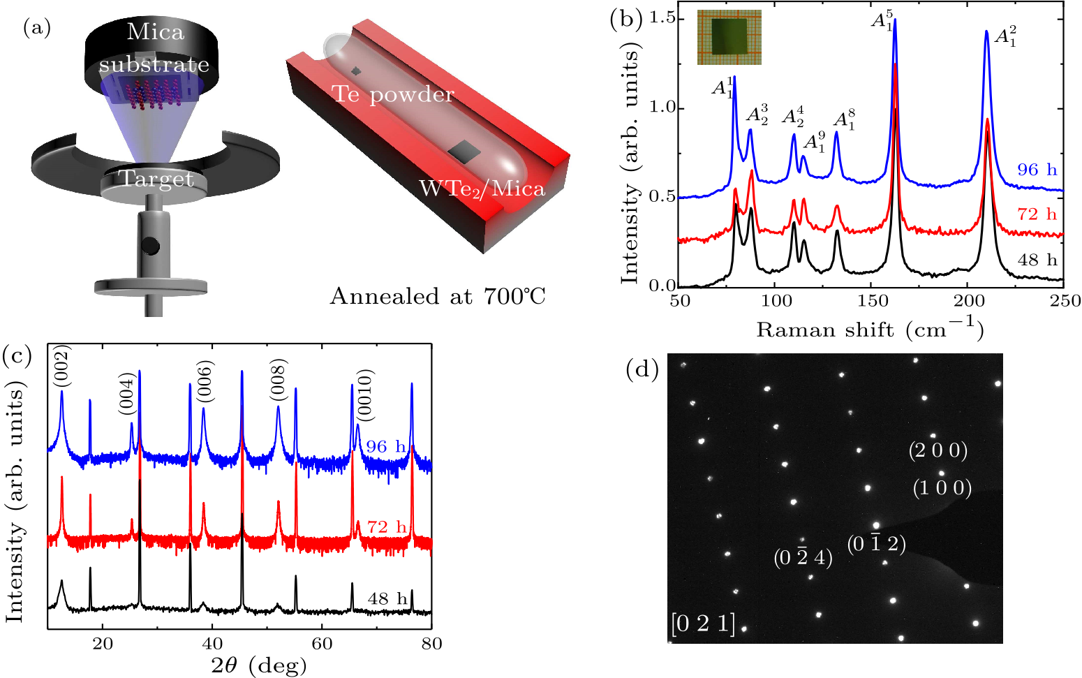
Citation Text: Chen Y Q, Chen Y D, Ning J A, Chen L M and Zhuang W Z et al 2020 Chin. Phys. Lett. 37 017104    Abstract Topological Weyl semimetal WTe$_{2}$ with large-scale film form has a promising prospect for new-generation spintronic devices. However, it remains a hard task to suppress the defect states in large-scale WTe$_{2}$ films due to the chemical nature. Here we significantly improve the crystalline quality and remove the Te vacancies in WTe$_{2}$ films by post annealing. We observe the distinct Shubnikov-de Haas quantum oscillations in WTe$_{2}$ films. The nontrivial Berry phase can be revealed by Landau fan diagram analysis. The Hall mobility of WTe$_{2}$ films can reach 1245 cm$^{2}$V$^{-1}$s$^{-1}$ and 1423 cm$^{2}$V$^{-1}$s$^{-1}$ for holes and electrons with the carrier density of $5\times 10^{19}$ cm$^{-3}$ and $2\times 10^{19}$ cm$^{-3}$, respectively. Our work provides a feasible route to obtain high-quality Weyl semimetal films for the future topological quantum device applications. DOI:10.1088/0256-307X/37/1/017104 PACS:71.18.+y, 71.20.Be, 73.50.Jt, 81.10.-h © 2020 Chinese Physics Society Article Text Shubnikov-de Haas (SdH) quantum oscillations in conductivity has become one of the most effective tools to explore novel physics in metals, semimetals and narrow-gap semiconductors since it was firstly discovered in bismuth in 1930.[1] It poses a way to describe the transport properties of related carriers close to Fermi surface.[2,3] Recently, the burgeoning topological quantum materials, such as topological insulators, Dirac semimetals and Weyl semimetals, have established a new state of condensed matter.[4–6] Unique electronic structures and strong spin-orbit coupling around Fermi surface bring them exotic physical properties, including unusually large magnetoresistance (MR)[7] and new nontrivial topological electronic state.[8] By analysis of SdH oscillations in these topological quantum materials, such as Bi$_{2}$Se$_{3}$[9] and Cd$_{3}$As$_{2}$,[10] the transport properties of relevant quasiparticles and their closed orbits at the Fermi surfaces can be thoroughly clarified. WTe$_{2}$, as a typical Weyl semimetal material, has type-II Weyl points resulted from the lack of inversion symmetry. It possesses a layered structure with an additional structural distortion along the crystallographic axis $a$ of tungsten chain.[11–13] Experimentally, it shows extremely unsaturated large MR of $\sim$13000000% in magnetic fields up to 60 T at 0.53 K.[11] Moreover, it has been demonstrated to own affluent Weyl features in three dimensions[14–17] and alluring topological quantum state in two dimensions.[18–22] Therefore, to elucidate the origin of these attractive physical properties, indispensable dissection based on the observed SdH oscillations is frequently implemented. Integration into the potential applications of spintronic devices and quantum computer, fabrication of smooth and continuous WTe$_{2}$ films is the first and very crucial step. The related fabrication techniques are chemical vapor deposition,[23–26] molecular beam epitaxy,[19,27,28] and pulsed laser deposition (PLD).[29–31] Despite great efforts have been devoted to achieving large-scale WTe$_{2}$ films, obtaining high-quality samples is of great difficulty due to the very low vapor pressure of cation tungsten. This limit prevents the observation of the typical SdH oscillations and/or other quantum effects in large-scale WTe$_{2}$ films. Thus, it still remains an urgent task to map the Fermi surface and its topology in continuously large-scale WTe$_{2}$ films. In this Letter, we fabricate the high-quality, large-scale, single-crystalline Weyl semimetal WTe$_{2}$ films on mica substrates by PLD and the post-annealing method. The SdH oscillations are observed in these WTe$_{2}$ films. According to the fast Fourier transform (FFT) and analysis of SdH quantum oscillations, the effective mass, the nontrivial Berry phase, the Dingle temperature, and the quantum mobility are determined. In addition, through two-carriers model fitting, the Hall mobility up to 1423 cm$^{2}$V$^{-1}$s$^{-1}$ is obtained, while the lower carrier density is achieved as compared to our previous work.[30] The WTe$_{2}$ target was prepared by the melting method.[30] The basic pressure of the PLD vacuum chamber was $\sim $$2.9\times 10^{-5}$ Pa and the distance between the substrate and the WTe$_{2}$ target was $\sim$5 cm, as shown in Fig. 1(a). The amorphous WTe$_{2}$ films were deposited onto the substrate at 300$^{\circ}\!$C at the speed of 1 nm/min for 100 min using a 248 nm KrF excimer laser beam (an average fluence of 1 J/cm$^{2}$ and a repetition rate of 2 Hz). Subsequently, an annealing process was implemented to crystallize the amorphous WTe$_{2}$ films. The films were sealed in a 20 mL evacuated quartz tube with 3.3 mg Te powder, and then were annealed at 700$^{\circ}\!$C for 48, 72 and 96 hours, respectively. Note that other annealing temperatures turned out the worse samples (see Fig. S1 in the Supplementary Material). The crystalline structure of these WTe$_{2}$ films was measured by a micro-Raman spectrometer (NT-MDT nanofinder-30) with a 514.5 nm Ar$^{+}$ laser and x-ray diffraction (XRD) using a Cu $K_\alpha$ line (Rigaku Ultima III). Selected area electron diffraction (SAED) attached in a transmission electron microscopy was used to confirm the single-crystalline nature. The thickness and surface morphology were examined by the atomic force microscope (AFM) system (Asylum Cypher) with the results shown Fig. S2 in the Supplementary Material. Furthermore, the films were cut into the size of $2.5\times 5\times 0.2$ mm$^{3}$ for the transport measurements, which was carried out in the standard Hall and resistivity configuration at low temperatures with a field up to 14 T (Oxford-14T). Standard lock-in amplifiers (Stanford Research System SR830) with a low frequency ($ < $20 Hz) excitation current of 1 µA (Keithley 6221) were used.
cpl-37-1-017104-fig1.png
Fig. 1. Structural characterization of the WTe$_{2}$ films. (a) Schematic diagrams of the PLD and annealing apparatus. (b) Raman spectra of the WTe$_{2}$ films annealed for different time intervals. Inset shows the digital photograph of the centimeter-scale WTe$_{2}$ film. (c) XRD patterns of the WTe$_{2}$ films annealed for different time intervals. The WTe$_{2}$ film is characterized as (00$l$) family diffraction peaks while the other peaks belong to the mica substrate. (d) The SAED pattern taken along the [021] zone axis of the WTe$_{2}$ film annealed for 72 hours.
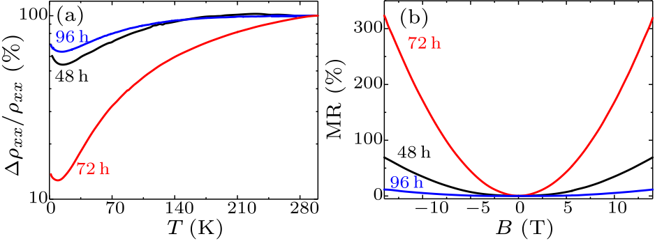
Figure 1(b) shows the Raman spectra of the WTe$_{2}$ films, which reveals seven main phonon peaks at about 79, 88, 110, 115, 132, 162, and 120 cm$^{-1}$, corresponding to $A_{1}^{1}$, $A_{2}^{3}$, $A_{2}^{4}$, $A_{1}^{9}$, $A_{1}^{8}$, $A_{1}^{5}$ and $A_{1}^{2}$ vibrational modes,[32] respectively. The XRD patterns exhibit diffraction peaks corresponding to (00$l$) family of planes [Fig. 1(c)], indicating the cleaved surface perpendicular to the $c$ axis of the WTe$_{2}$ films.[33] Notably, the XRD pattern of the WTe$_{2}$ films annealed for 48 hours has the widest full width at half maximum. In addition, the indiscernible diffraction peaks of (004) and (0010) for the 48-hour-annealed WTe$_{2}$ film indicate that the relatively fast annealing time (48 hours) suppresses the crystallization process. Furthermore, the SAED pattern further corroborates the single-crystalline nature of the WTe$_{2}$ film annealed for 72 hours [Fig. 1(d)]. The temperature-dependent longitudinal resistivity ($\rho_{xx}$) of WTe$_{2}$ films is displayed in Fig. 2(a), which is normalized by their values at 300 K. It is well-known that single-crystalline bulk WTe$_{2}$ has the well-defined metallic behavior.[11] Here, all the films show the metallic behavior beyond 15 K. Below 15 K, the low-temperature resistivity minima are visible, which are mainly attributed to the weak localization in quantum interference effects.[30] The residual resistivity ratios (RRRs, defined as RRR$\,= \frac{\rho_{\rm 300\,K}}{\rho_{\rm 1.7\,K}}$) of WTe$_{2}$ film annealed for 48, 72 and 96 hours are 1.75, 7.27 and 1.44, respectively. The RRR of WTe$_{2}$ film annealed for 96 hours is unexpectedly smaller than others, suggesting that the long annealing time may cause the existence of the much more content of Te vacancies in the WTe$_{2}$ films.[23,34] The MR curves (MR$\,= \frac{\rho (B)-\rho_{0}}{\rho_{0}}\times 100\%$) are shown in Fig. 2(b), where the external field is along the $c$ axis of the films. The WTe$_{2}$ film annealed for 72 (96) hours has the maximum (minimum) MR value of $\sim $321% (11%) at 14 T. This agrees well with our previous work that the Te deficiency in WTe$_{2}$ samples dramatically declines the MR value.[30] Moreover, according to the Lorentz law MR $\approx {{(\mu }_{\mathrm{avg}}\cdot B)}^{2}$, the average mobility of the WTe$_{2}$ films annealed for 48, 72 and 96 hours is calculated to be 621, 1347 and 248 cm$^{2}$V$^{-1}$s$^{-1}$, respectively. Therefore, the 48- and 96-hour-annealing duration suppresses the values of RRR and MR due to the incomplete crystallization as well as the much more Te vacancies.
cpl-37-1-017104-fig2.png
Fig. 2. (a) The temperature dependence of the longitudinal resistivity of the WTe$_{2}$ films annealed for different time intervals, as normalized by their values at 300 K. (b) The MR curves of the WTe$_{2}$ films annealed for different time intervals at 1.7 K.
cpl-37-1-017104-fig3.png
Fig. 3. (a) The MR curves of the WTe$_{2}$ film annealed for 72 hours at different temperatures. (b) Temperature dependence of SdH oscillations after a smooth subtraction of background. (c) The FFT of the SdH oscillations. Inset: the relationship between Landau level $n$ and the inverse field 1/$B$. (d) The temperature dependence of FFT amplitude at 175.4 T, as normalized by the value at 1.7 K. (e) The Dingle plot of the $\log(\Delta R\cdot B\cdot \sinh (\lambda Tm^*/B)/R)$ versus the inverse field 1/$B$ at 1.7 K.
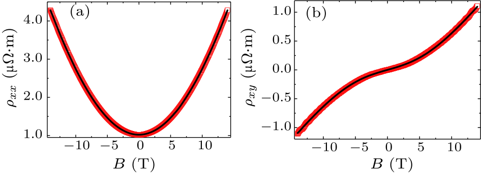
To clarify the transport properties of the WTe$_{2}$ film annealed for 72 hours, the dependence of the MR up to 14 T on temperature (from 1.7 to 100 K) is shown in Fig. 3(a). From 1.7 to 10 K, the MR value increases a little bit due to the faded weak localization component with increasing temperature.[30] Above 10 K, the MR value ordinarily decreases with increasing temperature due to the increased inelastic scattering,[35] i.e., electron-phonon scattering. Remarkably, the clear SdH oscillations periodic in 1/$B$ at temperatures between 1.7 and 10 K are extracted in Fig. 3(b) after a smooth subtraction of background. The FFT spectra of the SdH oscillations at temperatures between 1.7 and 10 K are shown in Fig. 3(c). It reveals a single oscillation frequency $F =175.4$ T of the SdH oscillations. According to the Onsager relation $F = ({\hbar}/2\pi e)A_{\rm F}$, where $\hbar$ is reduced Planck's constant and $A_{\rm F}$ is the cross-sectional area of this Fermi pocket normal to the field, $A_{\rm F}$ is determined to be $\sim $0.017 Å$^{-2}$. Furthermore, the Fermi wave vector $k_{\rm F} = 0.074$ Å$^{-1}$ can be acquired by a circular cross-sectional approximation. Landau fan diagram is shown in the inset of Fig. 3(c), where the minimum of $-d^{2}G_{xx}/d^{2}B$ ($G_{xx}$ is defined as $\frac{R_{xx}}{R_{xx}^{2}+R_{xy}^{2}}$) is chosen as the integral number of Landau level. Linear fitting line gives a nonzero intercept of $\sim $0.452, corresponding to a nontrivial Berry phase of $\pi$. In addition, the slope of this fitting line can also be described by the semiclassical Onsager equation: $k_{n \sim 1/ B}=A_{\rm F}\cdot{\hbar}/2\pi e$,[36] which results in the range of Landau fan diagram from 13.5 to 17. Generally, the SdH quantum oscillations can be described by the Lifshitz–Kosevich (LK) formula. The temperature dependence of the FFT amplitude can be defined as $$ A_{\mathrm{FFT}}\sim \Delta R\propto \frac{\lambda \cdot T\cdot m^{\ast }/B}{\sinh (\lambda \cdot T\cdot m^{\ast }/B)},~~ \tag {1} $$ where the $A_{\mathrm{FFT}}$ is the FFT amplitude, $\lambda = 2\pi^{2}k_{\rm B}/{\hbar}e$ ($k_{\rm B}$ is the Boltzmann constant), $T$ is the temperature, $m^{\ast}$ is the effective mass, and the 1/$B$ is the average inverse field of the Fourier window.[33] In Fig. 3(d), temperature dependence of the FFT amplitudes is normalized by their 1.7 K values. The black fitting line provides the effective mass of $\sim $$0.3605 m_{\rm e}$, comparable to those of high-quality exfoliated samples.[33] The Fermi velocity $v_{\rm F} = {\hbar}k_{\rm F}/m^{\ast}$ and the Fermi energy $E_{\rm F} = ({\hbar}k_{\rm F})^{2}/m^{\ast}$ are $\sim $$2.35 \times 10^{5}$ m/s and $\sim $113 meV, respectively. The Dingle plot of the $\log(\Delta R\cdot B\cdot \sinh (\lambda Tm^*/B)/R)$ versus the inverse field 1/$B$ is shown in Fig. 3(e). According to the slope $k\ln10 = -2\pi^{2}k_{\rm B}T_{\rm D}m^{\ast} /\hbar e$ of the linear fitting line, we can extract the Dingle temperature $T_{\rm D}$ of $\sim $4.74 K. Thereafter, the quantum scattering time $\tau = \hbar/ 2\pi k_{\rm B}T_{\rm D}$ is calculated to be $2.57 \times 10^{-13}$ s, so that the quantum mobility $\mu_{\rm q}=e\cdot\tau /m^{\ast}$ is $\sim $1249 cm$^{2}$V$^{-1}$s$^{-1}$. A mean free path of $l_{\rm q} = 60.4$ nm is estimated by the relation $l_{\rm q}=v_{\rm F}\cdot\tau$, which is comparable to those of other topological semimetals.[37–39] In WTe$_{2}$, the Fermi level is located at both conduction and valence bands simultaneously, which makes two kinds of carriers (electrons and holes) existing at the Fermi surface.[11] The nonlinear trend of Hall resistivity shown in Fig. 4 further proves the existence of electrons and holes in our WTe$_{2}$ films. To gain the Hall mobility and density of electrons and holes, the two-carrier model is used to fit the magnetic-field dependent magneto-resistivity $\rho_{xx}$ and Hall resistivity $\rho_{xy}$ at 1.7 K simultaneously:[40] $$ \rho_{xx}=\frac{1}{e}\frac{(p\mu_{\rm h}+n\mu_{\rm e})+(p\mu_{\rm h}\mu_{\rm e}^{2}+n\mu_{\rm e}\mu_{\rm h}^{2})B^{2}}{(p\mu_{\rm h}+n\mu_{\rm e})^{2}+(p-n)^{2}\mu_{\rm h}^{2}\mu_{\rm e}^{2}B^{2}},~~ \tag {2} $$ $$ \rho_{xy}=\frac{B}{e}\frac{(p\mu_{\rm h}^{2}-n\mu_{\rm e}^{2})+(p-n)\mu_{\rm h}^{2}\mu_{\rm e}^{2}B^{2}}{(p\mu_{\rm h}+n\mu_{\rm e})^{2}+(p-n)^{2}\mu_{\rm h}^{2}\mu_{\rm e}^{2}B^{2}},~~ \tag {3} $$ where $p$ and $n$ represent the density of holes and electrons, respectively; $\mu_{\rm h}$ and $\mu_{\rm e}$ are the Hall mobility of holes and electrons, respectively. Here, we obtain $p = 5 \times 10^{19}$ cm$^{-3}$ and $n = 2 \times 10^{19}$ cm$^{-3}$. Actually, the density of holes and electrons should be perfectly compensated in WTe$_{2}$. However, considering the existence of the Te vacancies, it is expected that there is a difference between the densities of holes and electrons. The $\mu_{\rm h}$ and $\mu_{\rm e}$ are calculated to be $\sim $1245 and 1423 cm$^{2}$V$^{-1}$s$^{-1}$, respectively. It should be noted that the quantum mobility (1249 cm$^{2}$V$^{-1}$s$^{-1}$) is comparable to the Hall mobility (1245 and 1423 cm$^{2}$V$^{-1}$s$^{-1}$).[38,41] This is due to the fact that the Te vacancies become the scattering centers which significantly reduce the MR and the Hall mobility. Compared with our previous work (average mobility of $\sim $730 cm$^{2}$V$^{-1}$s$^{-1}$ and carrier density of $\sim $10$^{20}$ cm$^{-3}$),[30] the mobility here is almost doubled while the carrier density decreases in an order. This remarkable improvement of quality makes the more balanced p–n compensation and suppresses the relevant inelastic scatting of carriers, enabling the SdH oscillations emergent in the high-quality WTe$_{2}$ films.
cpl-37-1-017104-fig4.png
Fig. 4. Field-dependent longitudinal resistivity (a) and Hall resistivity (b) of the WTe$_{2}$ film annealed for 72 hours at 1.7 K. The black lines are the fitting curves by the two-carries model.
In summary, we have fabricated the large-scale, high-quality, single-crystalline WTe$_{2}$ films on mica by the PLD and post-annealing method. The crystallization quality and the transport properties can be manipulated by tuning the annealing temperature and time. When the film is annealed at 700$^{\circ}\!$C for 72 hours, the distinct SdH oscillations are observed. Using the FFT and two-carriers model, physical quantities related to Fermi surface, such as the effective mass, nontrivial Berry phase, Dingle temperature, mobility and carrier density, are obtained. It is the doubled mobility and decreased carrier density that enable the observation of SdH quantum oscillations for the first time in the large-scale WTe$_{2}$ films. Our work raises the development of large-area topological film materials to a new stage, which provides a fertile land for the fabrication of the large-scale quantum devices based on Weyl materials.
References Fermi pockets and quantum oscillations of the Hall coefficient in high-temperature superconductorsComprehensive search for topological materials using symmetry indicatorsCatalogue of topological electronic materialsA complete catalogue of high-quality topological materialsExtremely large magnetoresistance and ultrahigh mobility in the topological Weyl semimetal candidate NbPTopological insulators in Bi2Se3, Bi2Te3 and Sb2Te3 with a single Dirac cone on the surfaceProbing the surface states in Bi 2 Se 3 using the Shubnikov–de Haas effectAngular-Dependent Phase Factor of Shubnikov–de Haas Oscillations in the Dirac Semimetal Cd 3 As 2 Large, non-saturating magnetoresistance in WTe2Anomalous Phase Shift of Quantum Oscillations in 3D Topological Semimetals3D Quantum Hall Effect of Fermi Arcs in Topological SemimetalsElectronic Structure Basis for the Extraordinary Magnetoresistance in WTe 2 Superconductivity emerging from a suppressed large magnetoresistant state in tungsten ditelluridePressure-driven dome-shaped superconductivity and electronic structural evolution in tungsten ditellurideGate-tunable negative longitudinal magnetoresistance in the predicted type-II Weyl semimetal WTe2Edge conduction in monolayer WTe2Quantum spin Hall state in monolayer 1T'-WTe2Observation of the quantum spin Hall effect up to 100 kelvin in a monolayer crystalElectrically tunable low-density superconductivity in a monolayer topological insulatorInterface-Induced High-Temperature Superconductivity in Single Unit-Cell FeSe Films on SrTiO3Tunable Positive to Negative Magnetoresistance in Atomically Thin WTe 2A library of atomically thin metal chalcogenidesCentimeter-Scale, Large-Area, Few-Layer 1T′-WTe 2 Films by Chemical Vapor Deposition and Its Long-Term Stability in Ambient ConditionLarge-Area and High-Quality 2D Transition Metal TellurideMagnetic Field Enhanced Superconductivity in Epitaxial Thin Film WTe2Direct visualization of a two-dimensional topological insulator in the single-layer 1 T WT e 2 Production of large-area 2D materials for high-performance photodetectors by pulsed-laser depositionTuning the transport behavior of centimeter-scale WTe 2 ultrathin films fabricated by pulsed laser depositionLow temperature epitaxy of tungsten–telluride heterostructure filmsRaman scattering investigation of large positive magnetoresistance material WTe 2Drastic Pressure Effect on the Extremely Large Magnetoresistance in WTe 2 : Quantum Oscillation StudyDramatically decreased magnetoresistance in non-stoichiometric WTe2 crystalsRoom Temperature Giant and Linear Magnetoresistance in Topological Insulator Bi 2 Te 3 NanosheetsThe Unique Current-Direction Dependent On-Off Switching in BiSbTeSe2 Topological Insulator Based Spin Valve TransistorsElectrical transport and optical properties of Cd 3 As 2 thin filmsQuantum oscillation and nontrivial transport in the Dirac semimetal Cd 3 As 2 nanodeviceMagneto-Transport and Shubnikov–de Haas Oscillations in the Type–II Weyl Semimetal Candidate NbIrTe 4 FlakeMagnetoresistance and quantum oscillations of an electrostatically tuned semimetal-to-metal transition in ultrathin WTe 2 Large linear magnetoresistance in the Dirac semimetal TlBiSSe
[1]Schubnikow L and Haas W J d 1930 Proc. Neth. R. Acad. Sci. 33 130
[2]Shoenberg D 2009 Magnetic Oscillations in Metals (Cambridge: Cambridge University Press)
[3] Chakravarty S and Kee H Y 2008 Proc. Natl. Acad. Sci. USA 105 8835
[4] Tang F, Po H C, Vishwanath A et al 2019 Nature 566 486
[5] Zhang T, Jiang Y, Song Z et al 2019 Nature 566 475
[6] Vergniory M G, Elcoro L, Felser C et al 2019 Nature 566 480
[7] Shekhar C, Nayak A K, Sun Y et al 2015 Nat. Phys. 11 645
[8] Zhang H, Liu C X , Qi X L et al 2009 Nat. Phys. 5 438
[9] Petrushevsky M, Lahoud E, Ron A et al 2012 Phys. Rev. B 86 045131
[10] Xiang Z J, Zhao D, Jin Z et al 2015 Phys. Rev. Lett. 115 226401
[11] Ali M N, Xiong J, Flynn S et al 2014 Nature 514 205
[12] Wang C M, Lu H Z and Shen S Q 2016 Phys. Rev. Lett. 117 077201
[13] Wang C M, Sun H P, Lu H Z et al 2017 Phys. Rev. Lett. 119 136806
[14] Pletikosic I, Ali M N, Fedorov A V et al 2014 Phys. Rev. Lett. 113 216601
[15] Kang D, Zhou Y, Yi W et al 2015 Nat. Commun. 6 7804
[16] Pan X C, Chen X, Liu H et al 2015 Nat. Commun. 6 7805
[17] Wang Y, Liu E, Liu H et al 2016 Nat. Commun. 7 13142
[18] Fei Z Y, Palomaki T, Wu S F et al 2017 Nat. Phys. 13 677
[19] Tang S J, Zhang C F, Wong D et al 2017 Nat. Phys. 13 683
[20] Wu S F, Fatemi V, Gibson Q D et al 2018 Science 359 76
[21] Fatemi V, Wu S F, Cao Y et al 2018 Science 362 926
[22] Sajadi E, Palomaki T, Fei Z Y et al 2018 Science 362 922
[23] Zhang E, Chen R, Huang C et al 2017 Nano Lett. 17 878
[24] Zhou J, Lin J, Huang X et al 2018 Nature 556 355
[25] Li J, Cheng S, Liu Z et al 2018 J. Phys. Chem. C 122 7005
[26] Zhou J, Liu F, Lin J et al 2017 Adv. Mater. 29 1603471
[27] Asaba T, Wang Y, Li G et al 2018 Sci. Rep. 8 6520
[28] Jia Z Y , Song Y H , Li X B et al 2017 Phys. Rev. B 96 041108
[29] Yao J D, Zheng Z Q and Yang G W 2019 Prog. Mater. Sci. 106 100573
[30] Gao M, Zhang M H, Niu W et al 2017 Appl. Phys. Lett. 111 031906
[31] Vermeulen P A, Momand J and Kooi B J 2019 CrystEngComm 21 3409
[32] Kong W D, Wu S F , Richard P et al 2015 Appl. Phys. Lett. 106 081906
[33] Cai P L, Hu J, He L P et al 2015 Phys. Rev. Lett. 115 057202
[34] Lv Y Y, Zhang B B, Li X et al 2016 Sci. Rep. 6 26903
[35] Wang X, Du Y, Dou S et al 2012 Phys. Rev. Lett. 108 266806
[36] Zhang M H, Wang X F, Zhang S et al 2016 IEEE Electron Device Lett. 37 1231
[37] Yang Y K , Xiu F X , Wang F Q et al 2019 Chin. Phys. B 28 107502
[38] Pan H, Zhang K, Wei Z et al 2016 Appl. Phys. Lett. 108 183103
[39] Huang X W , Liu X X , Yu P et al 2019 Chin. Phys. Lett. 36 077101
[40] Fatemi V, Gibson Q D, Watanabe K et al 2017 Phys. Rev. B 95 041410
[41] Novak M, Sasaki S, Segawa K et al 2015 Phys. Rev. B 91 041203