Chinese Physics Letters, 2019, Vol. 36, No. 9, Article code 097301 The 2D InSe/WS$_2$ Heterostructure with Enhanced Optoelectronic Performance in the Visible Region * Lu-Lu Yang (杨露露)1, Jun-Jie Shi (史俊杰)2, Min Zhang (张敏)3, Zhong-Ming Wei (魏钟鸣)4, Yi-Min Ding (丁一民)2, Meng Wu (吴蒙)2, Yong He (贺勇)3, Yu-Lang Cen (岑育朗)2, Wen-Hui Guo (郭文惠)2, Shu-Hang Pan (潘书航)2, Yao-Hui Zhu (朱耀辉)1** Affiliations 1Physics Department, Beijing Technology and Business University, Beijing 100048 2State Key Laboratory for Artificial Microstructures and Mesoscopic Physics, School of Physics, Peking University, Beijing 100871 3College of Physics and Electronic Information, Inner Mongolia Normal University, Hohhot 010022 4State Key Laboratory of Superlattices and Microstructures, Institute of Semiconductors, Chinese Academy of Sciences & College of Materials Science and Opto-Electronic Technology, University of Chinese Academy of Sciences, Beijing 100083 Received 12 January 2019, online 23 August 2019 *Supported by the National Natural Science Foundation of China under Grant Nos 11404013, 11474012, 11364030, 61622406, 61571415, 51502283 and 11605003, the National Key Research and Development Program of China under Grant No 2017YFA0206303, the MOST of China, and the 2018 Graduate Research Program of Beijing Technology and Business University.
**Corresponding author. Email: yaohuizhu@gmail.com
Citation Text: Yang L L, Shi J J, Zhang M, Wei Z M and Ding Y M et al 2019 Chin. Phys. Lett. 36 097301    Abstract Two-dimensional (2D) InSe and WS$_2$ exhibit promising characteristics for optoelectronic applications. However, they both have poor absorption of visible light due to wide bandgaps: 2D InSe has high electron mobility but low hole mobility, while 2D WS$_2$ is on the contrary. We propose a 2D heterostructure composed of their monolayers as a solution to both problems. Our first-principles calculations show that the heterostructure has a type-II band alignment as expected. Consequently, the bandgap of the heterostructure is reduced to 2.19 eV, which is much smaller than those of the monolayers. The reduction in bandgap leads to a considerable enhancement of the visible-light absorption, such as about fivefold (threefold) increase in comparison to monolayer InSe (WS$_2$) at the wavelength of 490 nm. Meanwhile, the type-II band alignment also facilitates the spatial separation of photogenerated electron-hole pairs; i.e., electrons (holes) reside preferably in the InSe (WS$_2$) layer. As a result, the two layers complement each other in carrier mobilities of the heterostructure: the photogenerated electrons and holes inherit the large mobilities from the InSe and WS$_2$ monolayers, respectively. DOI:10.1088/0256-307X/36/9/097301 PACS:73.22.-f, 73.63.-b, 78.67.-n © 2019 Chinese Physics Society Article Text In the past decade, many researchers have turned their attention to 2D semiconductors, such as transition-metal dichalcogenides ($MX_2$; $M$=Mo, W; $X$=S, Se, Te)[1,2] and group-III monochalcogenides ($MX$; $M$=Ga, In; $X$=S, Se, Te).[3,4] Studies on 2D semiconductors have demonstrated their advantages over the corresponding bulk materials in various optoelectronic applications.[5] Recently, 2D InSe has exhibited great potential for optoelectronic applications due to its high electron mobility, good metal contacts, and wide bandgap range.[6,7] The bandgap increases from 1.26 eV to 2.6 eV as bulk InSe is thinned to a monolayer.[7–9] The electron mobility of few-layer InSe exceeds $10^3$ cm$^2$V$^{-1}$s$^{-1}$ and $10^4$ cm$^2$V$^{-1}$s$^{-1}$ at room temperature and at liquid-helium temperature, respectively.[7] However, the optoelectronic properties of monolayer InSe need to be improved before it can be exploited widely in practice. First, its monolayer has a poor absorption of visible light due to the wide bandgap.[10] As a result, the performance of optoelectronic devices based on it would be reduced significantly in the visible region. Second, its hole mobility is rather low, although it has a large electron mobility. This severely impedes its applications in some types of optoelectronic devices; e.g., photoconductors and photodiodes. Fortunately, it has been shown that there is a unifying strategy to overcome both the difficulties; i.e., the construction of van der Waals (vdW) heterostructures with type-II band alignment.[11–14] The present work aims to enhance the optoelectronic performance of 2D InSe by combining it with another suitable 2D material to build a heterostructure. One of its possible counterparts is 2D WS$_2$, which also has a hexagonal structure.[15–18] Researchers have investigated its various applications, such as photocatalysis and optoelectronics.[19–24] Several heterostructures of WS$_2$ and other 2D materials have been fabricated and characterized experimentally.[15,24] In this Letter, we study the optoelectronic properties of the 2D InSe/WS$_2$ heterostructure by first-principles calculations before it is fabricated in experiments. The computational methods are outlined as follows: our first-principles calculations were performed with the Vienna ab initio simulation package.[25] Within the framework of the density functional theory, we use the generalized gradient approximation (GGA) with the Perdew–Burke–Ernzerhof (PBE) functional to describe the exchange and correlation interactions between the valence electrons.[26] The electron-ion interactions are described by the projector augmented-wave method.[27] Then, the GGA-1/2 scheme is used to make corrections to the band structures and optical properties, since the usual GGA underestimates bandgaps.[28] The GGA-1/2 scheme can yield the results in good agreement with experiments and with other theoretical methods such as the GW and HSE06 schemes. Meanwhile, this scheme is much less expensive than other computational methods. Within the GGA-1/2 scheme, the atomic self-energy potential is expressed as the difference between the all-electron potentials of the atom and those of the half-ion, $$ V_{\rm s}\approx{V}(0,r)-V(-1/2,r),~~ \tag {1} $$ where $r$ is the radial coordinate. The potential $V_{\rm s}$ has a long-range Coulomb tail that must be trimmed by $$ {\it \Theta}(r)=\begin{cases}\!\! \left[1-\left(\dfrac{r}{r_{\rm CUT}}\right)^m\right]^3,&~~r\leq{r_{\rm CUT}}; \\\!\! 0,&~~r>r_{\rm CUT}. \end{cases}~~ \tag {2} $$ The values of the dimensionless parameter $m$ and the trimming radius $r_{\rm CUT}$ are chosen to ensure that the result of the bandgap reaches its extreme. In optimizing geometric structures, the vdW interaction is accounted for by the optB88 vdW exchange functional.[29] We determine the positions of the conduction band minimum (CBM) and the valence band maximum (VBM) using the equation proposed by Toroker et al., $E_{\rm CBM/VBM}=E_{\rm BGC}\pm{E}_{\rm g}^{\rm QP}/2$, where $E_{\rm BGC}$ denotes the bandgap center calculated with the PBE functional and it is insensitive to different exchange functionals.[30] The quasiparticle bandgap $E_{\rm g}^{\rm QP}$ can be calculated by the GGA-1/2 method. We calculate the optical absorption spectrum of the 2D InSe/WS$_2$ heterostructure, as well as those of monolayer InSe and WS$_2$ by writing the absorption coefficient $I(\omega)$ in terms of the frequency-dependent dielectric function.[31] Furthermore, the electron and hole mobilities at temperature $T$ are computed by the widely used formula[11,32] $$ \mu_{\rm 2D}=\frac{e\hbar^3C_{\rm 2D}}{k_{\rm B}Tm^\ast{m}_{\rm d}E_1^2},~~ \tag {3} $$ where $C_{\rm 2D}$ denotes the in-plane stiffness and $E_1$ is the deformation potential constant. Various effective masses are used in Eq. (3): $m^\ast$ is the effective mass in the transport direction; i.e., $m_x^\ast$ or $m_y^\ast$, and $m_{\rm d}=\sqrt{m_x^\ast{m}_y^\ast}$ gives the average one over the $x$ and $y$ directions.
cpl-36-9-097301-fig1.png
Fig. 1. The top and side views of the crystal structures.[33] (a) Monolayer InSe has a honeycomb lattice connected by Se–In–In–Se sequence. (b) Monolayer WS$_2$ also has a hexagonal configuration, with each W atom anchored by three pairs of S atoms by S–W–S sequence. One of the lattice vectors (thick solid-black arrows) of the InSe (WS$_2$) supercell makes an angle of 30$^{\circ}$ (23.4$^{\circ}$) to the horizontal lattice vector (parallel to the thin dashed-black line) of its primitive cell. (c) One (optimized) primitive cell of the 2D InSe/WS$_2$ heterostructure is composed of the supercells of the InSe and WS$_2$ monolayers shown in (a) and (b). One monolayer is stacked on the other by matching the rhombuses of their supercells until they coincide with each other. The optimized interlayer distance is $d=3.40$ Å in the heterostructure.
Table 1. The equilibrium lattice constants $a$ (in units of Å) and bandgaps $E_{\rm g}$ (in units of eV) of monolayer InSe and WS$_2$.
MLs $a$ $E_{\rm g}$ (PBE) $E_{\rm g}$ (GGA-1/2) $E_{\rm g}$ (GW) $E_{\rm g}$ (Exp.)
InSe 4.09 1.47 2.75 2.83$^{\rm a}$ 2.6$^{\rm c}$
WS$_2$ 3.19 1.77 2.59 2.64$^{\rm b}$ 2.38$^{\rm d}$
$^{\rm a}$From Ref.  [9], $^{\rm b}$From Ref.  [21], $^{\rm c}$From Ref.  [7], $^{\rm d}$From Ref.  [34].
The crystal structures of 2D InSe, WS$_2$, and InSe/WS$_2$ heterostructure are shown in Fig. 1. Our structural optimizations yield the lattice constants for InSe and WS$_2$ monolayers (listed in Table 1) and are in good agreement with the values in previous reports.[4,9,20,21,35–40] Because of the huge lattice mismatch (over $20$%) between the two pristine monolayers, we build a large cell for the 2D InSe/WS$_2$ heterostructure in such a way that the lattice mismatch is made as small as possible and the computational cost is still acceptable at the same time. As a reasonable compromise, we choose a primitive cell of the heterostructure consisting of two hexagonal supercells: a $\sqrt{12}\times \sqrt{12}$ supercell of InSe (24 In and 24 Se atoms) and a $\sqrt{19}\times \sqrt{19}$ supercell of WS$_2$ (19 W and 38 S atoms) as shown in Fig. 1. Then, one can find a lattice mismatch smaller than 1.7% by comparing $\sqrt{12}a_{\rm InSe}$ and $\sqrt{19}a_{\rm WS_2}$ in Fig. 1 and using the lattice constants listed in Table 1. Our structural optimization yields a lattice constant of 14.09 Å (the side length of the rhombus in Fig. 1(c)) for the heterostructure, which induces a compressive strain of 0.6% in the InSe monolayer and a tensile strain of 1.3% in the WS$_2$ monolayer. During the geometry optimization, the cell shape, cell volume, and ion positions are allowed to change automatically (ISIF=3) with the lattice vector perpendicular to the layer plane fixed (negligible stress due to the thick vacuum layer). We begin the optimizations with a series of initial interlayer distances (from 3.20 Å to 4.00 Å in increments of 0.10 Å) for the heterostructure, and all of them end up with the same equilibrium interlayer distance $d=3.40$ Å. The key computational parameters are outlined as follows: two $k$-point meshes, $5\times5\times1$ and $7\times7\times1$, are employed for the geometry optimizations and self-consistent calculations of the supercell, respectively. The thickness of the vacuum layer is over 20 Å so as to ensure decoupling between periodically repeated layers, and the energy cutoff is set to 450 eV. The structures are fully optimized until the residual atomic forces are smaller than 0.01 eV/Å. Moreover, we use the Gaussian smearing in combination with a reasonable smearing parameter, i.e., 0.05 and 0.1 for the monolayers and the heterostructure, respectively.
cpl-36-9-097301-fig2.png
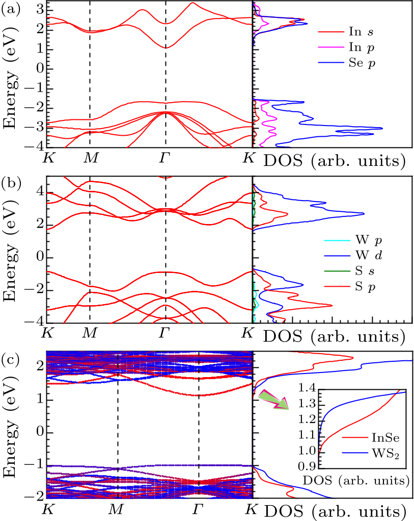
Fig. 2. Band structures and projected DOS. (a) Monolayer InSe has an indirect bandgap (2.75 eV) with the CBM located at ${\it \Gamma}$ point and the VBM located between ${\it \Gamma}$ and $K$ points. Its CBM (VBM) is mainly composed of Se 4$p$ and In 5$s$ (5$p$) orbitals. (b) Monolayer WS$_2$ has a direct bandgap of 2.59 eV with both its CBM and VBM located at $K$ points.[35] Its W 5$d$ orbitals play the dominant role in both the CBM and VBM, while its S 3$p$ orbitals make a minor contribution. (c) The weighted band structure and DOS of the InSe/WS$_2$ heterostructure. Its CBM is dominated by the InSe layer as shown by the inset.
The GGA-1/2 scheme is applied firstly to monolayer InSe and WS$_2$ to calibrate computational parameters. The bandgaps calculated with these parameters are quite reasonable as each of them falls between the corresponding GW result and that reported by experimental groups as listed in Table 1. The band structures and the corresponding density of states (DOS) of the two monolayers are shown in Figs. 2(a) and 2(b). The electronic properties of monolayer InSe and WS$_2$ are also consistent with the results of previous calculations.[9,21] The stability of the heterostructure is described by its binding energy $E_{\rm b}$. We write $E_{\rm b}$ as $E_{\rm b}=(E_{\rm InSe/WS_2}-E_{\rm InSe}-E_{\rm WS_2})/n$, where $n$ is the number of all types of atoms. Moreover, $E_{\rm InSe/WS_2}$, $E_{\rm InSe}$, and $E_{\rm WS_2}$ are the total energies of the relaxed heterostructure, monolayer InSe, and monolayer WS$_2$, respectively.[17] The calculated binding energy is $-30$ meV/atom for the heterostructure. This indicates a moderate interaction between the two monolayers and the heterostructure satisfies one of the requirements on a stable structure.
cpl-36-9-097301-fig3.png
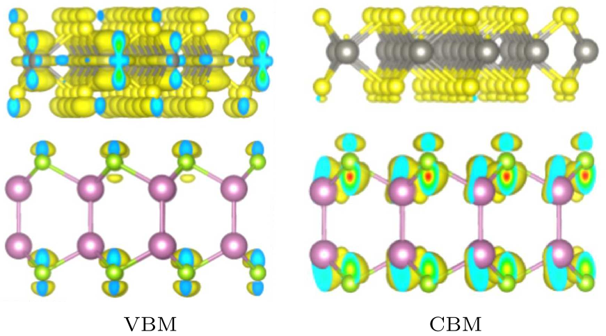
Fig. 3. The charge density at the VBM (CBM) depicted by the isosurface ($\rho=1.36\times10^{-4}\,e$Å$^{-3}$) in the heterostructure.
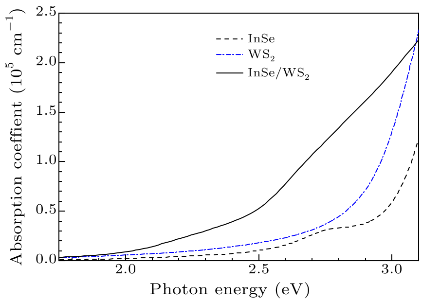
Figure 2(c) shows the weighted band structure and the corresponding DOS of the heterostructure. The bandgap of the InSe/WS$_2$ heterostructure is reduced to 2.19 eV, which is much smaller than those of monolayer InSe and WS$_2$ (see Table 1). This reduction will be interpreted qualitatively by the band edge alignment below. Figure 3 depicts the isosurface charge density at the VBM and the CBM of the heterostructure. The size of the isosurface indicates that an electron at the CBM resides almost entirely in the InSe layer. This is consistent with the band structure of the CBM and its DOS shown in Fig. 2(c), where the InSe layer is definitely dominant over the WS$_2$ layer. On the other hand, a hole at the VBM exhibits more complicated behavior. It has noticeable probability to appear in the InSe layer, although it resides mainly in the WS$_2$ layer. This is also in agreement with the band structure of the VBM and its DOS in Fig. 2(c), where the WS$_2$ layer plays a major role. Therefore, photogenerated electron-hole pairs can be effectively separated: electrons and holes reside preferably in the InSe and WS$_2$ layers, respectively. The InSe/WS$_2$ heterostructure has a type-II band alignment. The CBM and VBM of monolayer InSe are $-3.86$ eV and $-6.61$ eV, respectively, with respect to the vacuum level, which are in agreement with the previous results.[9] As for monolayer WS$_2$, the CBM and VBM are $-3.41$ eV and $-6.00$ eV, respectively, which are roughly consistent with the previous reports.[21] Both the CBM and the VBM of InSe are lower than those of WS$_2$. The conduction band offset (CBO) and the valence band offset (VBO) are 0.45 eV and 0.61 eV, respectively. Thus the heterostructure has a type-II band alignment, which is consistent with the electronic structures in Fig. 2(c). Straightforward calculation shows that the bandgap of the heterostructure is reduced to 2.14 eV, which is close to the more rigorous result (2.19 eV) given by the band structure in Fig. 2(c). The difference is attributed to the strain and interlayer interaction in the heterostructure. Figure 4 presents the optical absorption spectrum of the InSe/WS$_2$ heterostructure together with those of monolayer InSe and WS$_2$. In comparison to monolayer InSe and WS$_2$, the spectrum of the heterostructure has a much wider energy range, in which the absorption coefficient for visible light is on the order of 10$^5$ cm$^{-1}$. Specifically, its absorption coefficient has a nearly fivefold (threefold) enhancement for the photon energy 2.53 eV (the light wavelength of 490 nm) in comparison to monolayer InSe (WS$_2$). The enhanced light absorption is largely owing to the smaller bandgap of the heterostructure as shown in Fig. 2(c). It is worthwhile to point out that the bandgap will be reduced further if the exciton effects are taken into account. The first-principles calculation of the exciton binding energy ($E_{\rm eb}$) is usually very time-consuming and beyond the scope of the current work. Fortunately, it can be estimated using a robust linear scaling law, i.e., $E_{\rm eb}\approx{E}_{\rm g}/4$, for 2D semiconductors.[41] We obtain $E_{\rm eb}\approx0.55$ eV using this method, and then the optical bandgap is roughly 1.64 eV when $E_{\rm eb}$ is subtracted from the fundamental bandgap (2.19 eV). This will give rise to a remarkable exciton absorption peak far below the absorption edge in Fig. 4.
cpl-36-9-097301-fig4.png
Fig. 4. Absorption spectra of visible light. The solid-black, dash-dotted-blue, and dashed-black curves depict the variation of the absorption coefficients with photon energy for the InSe/WS$_2$ heterostructure, monolayer WS$_2$, and monolayer InSe, respectively.
Table 2. The electron and hole mobilities listed together with the associated coefficients for monolayer InSe, monolayer WS$_2$, and the 2D InSe/WS$_2$ heterostructure. Both $x$ and $y$ components are given for the effective masses $m^\ast$, deformation potential constants $E_1$, in-plane stiffness $C_{\rm 2D}$, and mobilities $\mu_{\rm 2D}$. Refer to Eq. (3) for details.
Carriers Materials $m_x^{\ast}$ $m_y^{\ast}$ $E_{1x}$ $E_{1y}$ $C_{{\rm 2D}-x}$ $C_{{\rm 2D}-y}$ $\mu_{{\rm 2D}-x}$ $\mu_{{\rm 2D}-y}$
InSe 0.18 0.19 $-$4.42 $-$4.32 49.47 48.70 1667 1584
Electrons WS$_{2}$ 0.45 0.33 $-$11.20 $-$11.80 145.79 148.51 122 179
InSe/WS$_{2}$ 0.23 0.24 $-$4.00 $-$4.10 182.53 185.21 4503 4168
InSe 1.84 2.01 $-$1.40 $-$1.37 49.47 48.70 152 143
Holes WS$_{2}$ 0.53 0.43 $-$5.19 $-$5.40 145.79 148.51 456 529
InSe/WS$_{2}$ 1.22 1.15 $-$3.48 $-$4.23 182.53 185.21 223 162
Table 2 lists the electron and hole mobilities of the heterostructure together with those of monolayer InSe and WS$_2$. There is a pronounced increase in the electron mobility of the heterostructure; i.e., nearly threefold increase in comparison to that of monolayer InSe. At the same time, the electron mobility of the heterostructure is much larger than that of the monolayer WS$_2$, which indicates that there is no close relationship between the two mobilities. The electron mobility is dominated by the contribution from the InSe layer since the photogenerated electrons almost reside in this layer as shown by the band structure in Fig. 2(c) and the CBM electron density in Fig. 3. This explains why the electron mobility of the WS$_2$ is not related to that of the heterostructure. The pronounced increase in the electron mobility of the heterostructure results from the large increase of the stiffness ($C_{{\rm 2D}-x(y)}$) relative to that of monolayer InSe.[42] The stiffness of the heterostructure is roughly equal to the sum of those of InSe and WS$_2$ monolayers. Moreover, the heterostructure effects are dominant over the correction due to the finite thickness, since the structure studied here is rather thin.[43] The mobility of the holes exhibits more complicated characteristics than that of the electrons. The hole mobility of the heterostructure increases remarkably in comparison to that of monolayer InSe while it decreases significantly as compared with that of monolayer WS$_2$. The photogenerated holes reside mostly in the WS$_2$ layer and partly in the InSe layer as shown by the band structure in Fig. 2(c) and the VBM electron density in Fig. 3. This is consistent with the change in the hole effective mass of the heterostructure listed in Table 2; i.e., the hole effective mass falls between the values of the InSe and the WS$_2$ layers. Meanwhile, $E_{\rm 1x(y)}$ also exhibits the similar variation. As compared with monolayer InSe, $m_{x(y)}^\ast$ of the heterostructure decreases and tends to increase the hole mobility, while $E_{1x(y)}$ increases in magnitude and makes the hole mobility smaller instead. The two variations cancel each other partly in the contribution to the hole mobility. However, the hole mobility has an overall increase in comparison to that of the InSe layer when the large increase in the stiffness is taken into account. In summary, our first-principles calculations show that the 2D InSe/WS$_2$ heterostructure exhibits enhanced optoelectronic performance in the visible region. It has a type-II band alignment and its bandgap is reduced to 2.19 eV. Its CBM and VBM derive mainly from the InSe and WS$_2$ layers, respectively, which promotes effectively the spatial separation of the photogenerated electron-hole pairs and in turn decreases their recombination rate. The visible-light absorption is increased considerably in comparison to monolayer InSe (WS$_2$). The two monolayers complement each other in carrier mobilities: the photo-generated electrons and holes inherit the large mobilities from InSe and WS$_2$ monolayers, respectively. The results presented here may be useful for experimentalists working on this structure.
References Electronics and optoelectronics of two-dimensional transition metal dichalcogenidesThe chemistry of two-dimensional layered transition metal dichalcogenide nanosheetsSynthesis, properties and applications of 2D layered M III X VI (M = Ga, In; X = S, Se, Te) materials2D layered group IIIA metal chalcogenides: synthesis, properties and applications in electronics and optoelectronicsGraphene-Like Two-Dimensional MaterialsBack Gated Multilayer InSe Transistors with Enhanced Carrier Mobilities via the Suppression of Carrier Scattering from a Dielectric InterfaceHigh electron mobility, quantum Hall effect and anomalous optical response in atomically thin InSeTuning the Bandgap of Exfoliated InSe Nanosheets by Quantum ConfinementSingle-Layer Group-III Monochalcogenide Photocatalysts for Water SplittingStrain induced new phase and indirect–direct band gap transition of monolayer InSeEnhancement of hole mobility in InSe monolayer via an InSe and black phosphorus heterostructureFast, multicolor photodetection with graphene-contacted p -GaSe/ n -InSe van der Waals heterostructuresElectronic properties of silicene in BN/silicene van der Waals heterostructuresTwo-dimensional g-C 3 N 4 /InSe heterostructure as a novel visible-light photocatalyst for overall water splitting: a first-principles studyStrain engineering in monolayer WS 2 , MoS 2 , and the WS 2 /MoS 2 heterostructureDFT investigation on two-dimensional GeS/WS2 van der Waals heterostructure for direct Z-scheme photocatalytic overall water splittingC2N/WS2 van der Waals type-II heterostructure as a promising water splitting photocatalystHybrid density functional study on the photocatalytic properties of AlN/MoSe 2 , AlN/WS 2 , and AlN/WSe 2 heterostructuresTwo-Dimensional Nanosheets Produced by Liquid Exfoliation of Layered MaterialsPhotosensor Device Based on Few-Layered WS 2 FilmsComputational Search for Single-Layer Transition-Metal Dichalcogenide PhotocatalystsElectrical Transport Properties of Single-Layer WS 2Vertically Aligned WS 2 Nanosheets for Water SplittingMoS 2 /WS 2 Heterojunction for Photoelectrochemical Water OxidationEfficient iterative schemes for ab initio total-energy calculations using a plane-wave basis setGeneralized Gradient Approximation Made SimpleFrom ultrasoft pseudopotentials to the projector augmented-wave methodApproximation to density functional theory for the calculation of band gaps of semiconductorsVan der Waals density functionals applied to solidsFirst principles scheme to evaluate band edge positions in potential transition metal oxide photocatalysts and photoelectrodesElectronic structure, chemical bonding, and optical properties of paraelectric BaTiO 3 High-mobility transport anisotropy and linear dichroism in few-layer black phosphorusVESTA 3 for three-dimensional visualization of crystal, volumetric and morphology dataElectronic band gaps and exciton binding energies in monolayer M o x W 1 x S 2 transition metal dichalcogenide alloys probed by scanning tunneling and optical spectroscopyThickness and strain effects on electronic structures of transition metal dichalcogenides: 2H- M X 2 semiconductors ( M = Mo, W; X = S, Se, Te)Band offsets and heterostructures of two-dimensional semiconductorsStrain engineering of WS 2 , WSe 2 , and WTe 2Electronic structures and elastic properties of monolayer and bilayer transition metal dichalcogenides MX 2 ( M = Mo, W; X = O, S, Se, Te): A comparative first-principles studyTwo-Dimensional Indium Selenides Compounds: An Ab Initio StudyComputational mining of photocatalysts for water splitting hydrogen production: two-dimensional InSe-family monolayersScaling Universality between Band Gap and Exciton Binding Energy of Two-Dimensional SemiconductorsFew-layer Tellurium: one-dimensional-like layered elementary semiconductor with striking physical properties
[1] Wang Q H et al 2012 Nat. Nanotechnol. 7 699
[2] Chhowalla M et al 2013 Nat. Chem. 5 263
[3] Xu K et al 2016 Nanoscale 8 16802
[4] Huang W et al 2016 CrystEngComm 18 3968
[5] Xu M, Liang T, Shi M and Chen H 2013 Chem. Rev. 113 3766
[6] Feng W, Zheng W, Cao W and Hu P 2014 Adv. Mater. 26 6587
[7] Bandurin D A et al 2017 Nat. Nanotechnol. 12 223
[8] Mudd G W et al 2013 Adv. Mater. 25 5714
[9] Zhuang H L and Hennig R G 2013 Chem. Mater. 25 3232
[10] Hu T, Zhou J and Dong J 2017 Phys. Chem. Chem. Phys. 19 21722
[11] Ding Y M et al 2017 Nanoscale 9 14682
[12] Yan F et al 2017 Nanotechnology 28 27LT01
[13] Wu Z B et al 2018 Chin. Phys. B 27 077302
[14] He Y et al 2019 J. Phys. D 52 015304
[15] He X et al 2016 Appl. Phys. Lett. 109 173105
[16] Ju L et al 2018 Appl. Surf. Sci. 434 365
[17] Kumar R, Das D and Singh A K 2018 J. Catal. 359 143
[18] Wang G et al 2018 J. Phys. D 51 025109
[19] Coleman J N et al 2011 Science 331 568
[20] PereaL ópez N et al 2013 Adv. Funct. Mater. 23 5511
[21] Zhuang H L and Hennig R G 2013 J. Phys. Chem. C 117 20440
[22] Ovchinnikov D et al 2014 ACS Nano 8 8174
[23] Yang Y et al 2015 Adv. Funct. Mater. 25 6199
[24] Pesci F M et al 2017 ACS Catal. 7 4990
[25] Kresse G and Furthmüller J 1996 Phys. Rev. B 54 11169
[26] Perdew J P, Burke K and Ernzerhof M 1996 Phys. Rev. Lett. 77 3865
[27] Kresse G and Joubert D 1999 Phys. Rev. B 59 1758
[28] Ferreira L G, Marques M and Teles L K 2008 Phys. Rev. B 78 125116
[29] Klimeš J, Bowler D R and Michaelides A 2011 Phys. Rev. B 83 195131
[30] Toroker M C et al 2011 Phys. Chem. Chem. Phys. 13 16644
[31] Saha S, Sinha T P and Mookerjee A 2000 Phys. Rev. B 62 8828
[32] Qiao J et al 2014 Nat. Commun. 5 4475
[33] Momma K and Izumi F 2011 J. Appl. Crystallogr. 44 1272
[34] Rigosi A F et al 2016 Phys. Rev. B 94 075440
[35] Yun W S et al 2012 Phys. Rev. B 85 033305
[36] Kang J et al 2013 Appl. Phys. Lett. 102 012111
[37] Amin B, Kaloni T P and Schwingenschlögl U 2014 RSC Adv. 4 34561
[38] Zeng F, Zhang W B and Tang B Y 2015 Chin. Phys. B 24 097103
[39] Debbichi L, Eriksson O and Lebègue S 2015 J. Phys. Chem. Lett. 6 3098
[40] Peng Q et al 2017 Catal. Sci. Technol. 7 2744
[41] Jiang Z et al 2017 Phys. Rev. Lett. 118 266401
[42]Kang P et al 2017 2D Mater. 4 045014
[43] Qiao J et al 2018 Sci. Bull. 63 159