Chinese Physics Letters, 2019, Vol. 36, No. 6, Article code 067502 Tunable Perpendicular Magnetic Anisotropy in Off-Stoichiometric Full-Heusler Alloy Co$_{2}$MnAl * Zhi-Feng Yu (余之峰)1,2, Jun Lu (鲁军)1,2, Hai-Long Wang (王海龙)1,2, Xu-Peng Zhao (赵旭鹏)1,2, Da-Hai Wei (魏大海)1,2, Jia-Lin Ma (马佳淋)1,2, Si-Wei Mao (毛思玮)1,2, Jian-Hua Zhao (赵建华)1,2,3** Affiliations 1State Key Laboratory of Superlattices and Microstructures, Institute of Semiconductors, Chinese Academy of Sciences, Beijing 100083 2Center of Materials Science and Optoelectronics Engineering, University of Chinese Academy of Sciences, Beijing 100190 3Beijing Academy of Quantum Information Sciences, Beijing 100193 Received 4 March 2019, online 18 May 2019 *Supported by the National Key Research and Development Program of China under Grant Nos 2017YFB0405701 and 2018YFB0407601, the National Natural Science Foundation of China under Grant Nos U1632264 and 11874349, and the Key Research Project of Frontier Science of the Chinese Academy of Sciences under Grant Nos QYZDY-SSW-JSC015 and XDPB12.
**Corresponding author. Email: jhzhao@red.semi.ac.cn
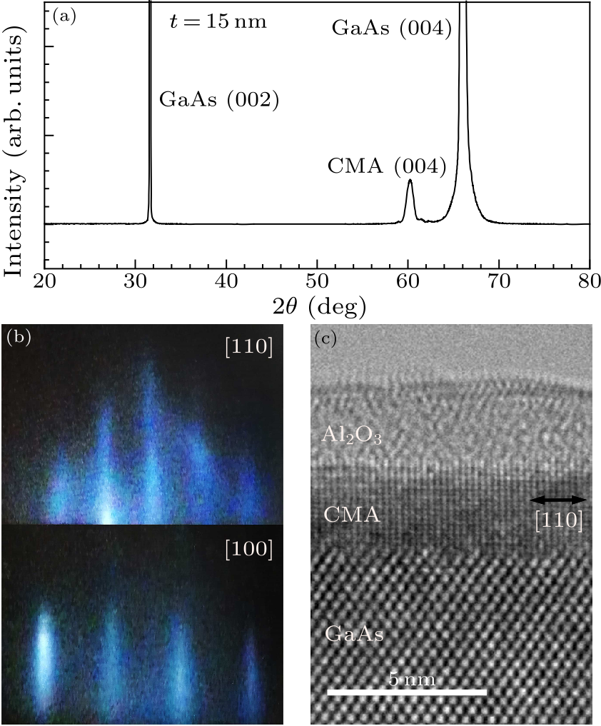
Citation Text: Yu Z F, Lu J, Wang H L, Zhao X P and Wei D H et al 2019 Chin. Phys. Lett. 36 067502    Abstract Off-stoichiometric full-Heusler alloy Co$_{2}$MnAl thin films with different thicknesses are epitaxially grown on GaAs (001) substrates by molecular-beam epitaxy. The composition of the films, close to Co$_{1.65}$Mn$_{1.35}$Al (CMA), is determined by x-ray photoelectron spectroscopy and energy dispersive spectroscopy. Tunable perpendicular magnetic anisotropy (PMA) from 3.41 Merg/cm$^{3}$ to 1.88 Merg/cm$^{3}$ with the thickness increasing from 10 nm to 30 nm is found, attributed to the relaxation of residual compressive strain. Moreover, comparing with the ultrathin CoFeB/MgO used in the conventional perpendicular magnetic tunnel junction, the CMA electrode has a higher magnetic thermal stability with more volume involved. The PMA in CMA films is sustainable up to 300$^{\circ}\!$C, compatible with semiconductor techniques. This work provides a possibility for the development of perpendicular magnetized full-Heusler compounds with high thermal stability and spin polarization. DOI:10.1088/0256-307X/36/6/067502 PACS:75.50.Cc, 75.30.Gw, 81.15.Hi © 2019 Chinese Physics Society Article Text Co-based full-Heusler alloys with composition Co$_{2}$YZ have attracted much attention in the ascendance of spintronics in recent years because of their half-metallicity and high Curie temperature.[1,2] Generally, the energy states of these ferromagnets at the Fermi level $\varepsilon_{_{\rm F}}$ are occupied by majority-spin electrons, while $\varepsilon_{_{\rm F}}$ lies within the gap of the minority-spin band, which brings 100% spin polarization at $\varepsilon_{_{\rm F}}$ theoretically.[3,4] In principle, the higher the spin polarization of the electrode in a magnetic tunnel junction (MTJ), the larger the tunneling magneto-resistance reached. Meanwhile, with the increasing requirements of scalability and low power consumption, magnetic materials with perpendicular magnetic anisotropy (PMA) are much more desirable. Hence, it is worth mentioning that full-Heusler alloys with PMA could be a promising candidate material family in various spintronic devices, such as spin transfer-torque magnetic random access memory[5,6] and spin-torque nano-oscillators.[7] However, Heusler alloys predominantly have cubic crystalline structures and possess in-plane magneto-crystalline anisotropy, which set a limitation for their practical applications. Thus a great deal of attention has been paid to the modulation of the magnetic anisotropy of Heusler alloys from the in-plane to the out-of-plane magnetization.[8] According to previous works, the PMA of full-Heusler alloys can be induced by the adjacent perpendicular magnetized film or seed layer with exchange coupling.[9,10] Moreover, Heusler alloys can also realize PMA in the heterostructure sandwiched by MgO and heavy metal.[11] Nevertheless, it is noted that the PMA in these Heusler alloys vanishes when the thickness exceeds a small value, which for example is 3 nm in $L$1-CoPt/Co$_{2}$MnSi,[10] indicating that the PMA of full-Heusler alloys mentioned above is more likely related to interface-induced effects. Co$_{2}$MnAl is a typical full-Heusler ferromagnet with cubic crystalline structure and in-plane magnetic easy axis.[2] To realize PMA in Co$_{2}$MnAl, lattice distortion is required and a feasible method is atomic substitution. Considering the existence of the lattice distortion in Mn$_{2}$CoAl,[12] a spin gapless semiconductor, it is possible to induce strain with excessive Mn partial substitution for Co. According to the previous work of calculations, the spin polarization still remains higher than 75% with such a stoichiometric deviation.[13] In addition, according to the calculated results, similar Heusler compounds Co$_{2}$MnX (X=Si, Ge, Sn) will sustain half-metallicity with a slight distortion ($ < 2$%) in the lattice constant.[3] Based on the motivations mentioned above, it will be meaningful if the off-stoichiometric full-Heusler alloy Co$_{2}$MnAl has PMA induced by residual strain. Furthermore, Co$_{1.65}$Mn$_{1.35}$Al (CMA) films are directly grown on GaAs substrates, making the system simpler than multilayer films and showing much potential in the integration of spintronics and semiconductor techniques. In the present work, the epitaxial single-crystalline films of CMA were grown on GaAs (001) substrates by molecular-beam epitaxy. After GaAs de-oxidation and buffer layer deposition, Mn, Co and Al atoms were co-deposited at room temperature for 1 min and annealed at 250$^{\circ}\!$C for 10 min. CMA thin films were then grown at 200$^{\circ}\!$C with different thicknesses of $t=2.5$, 10, 15, 20 and 30 nm which were determined by the x-ray reflectivity and transmission electron microscope (TEM) results as well as the growth time. Reflection high-energy electron diffraction (RHEED) was used to monitor the whole epitaxial growth in situ as shown in Fig. 1(b) indicating the single crystallization of the film. To protect the films from oxidation, 2-nm-thick aluminum was deposited on the samples.
cpl-36-6-067502-fig1.png
Fig. 1. (a) XRD $\theta$–$2\theta$ scans for a 15-nm-thick CMA film on a GaAs (001) substrate. (b) CMA RHEED patterns with electrons parallel to the [100] and [110] azimuths. (c) The TEM image of a 2.5-nm-thick CMA film.
The composition of the films is determined by x-ray photoelectron spectroscopy, which is coincident with the results measured by energy dispersive spectroscopy. The structure is analyzed by x-ray diffraction (XRD) and TEM. The magnetic properties are mainly measured using a superconducting quantum interference device at 280 K and fields up to 5 T. XRD scans are conducted in a $\theta$–$2\theta$ configuration with Cu $K_{\alpha}$ radiation at 1.5406 Å. Figure 1(a) shows the CMA (004) diffraction peak appearing on the smaller angle side of the GaAs (004) substrate peak. To reduce the probability of interfacial reaction and to maintain the residual strain in the film, the growth temperature is located at almost the lowest limit for crystallization fingerprinted by the RHEED patterns changing with annealing. Under the special growth conditions, our samples have an A2 structure confirmed by the absence of a CMA (002) peak, which is similar to that of the Co$_{2}$MnAl shown in the previous work.[14] Figure 1(b) shows the CMA RHEED patterns with a recurring period of 90$^{\circ}\!$, taken along the [100] and [110] azimuths, showing a four-fold symmetry of the structure. Moreover, the contrast between the spacing of the electron diffraction stripes taken along the [100] and [110] azimuths indicates that the epitaxial relationship can be determined as CMA (001) [100]$\parallel$GaAs (001) [100]. Limited to the measurement system, the lattice constant $a$ is determined by the TEM image. The projection of the atomic configuration of a 2.5-nm-thick sample is shown in Fig. 1(c), in which the distance between adjacent atoms of the CMA film projected on the (1$\bar{1}$0) plane is about 2 Å. According to the above analysis, the $a$ value of the 2.5-nm-thick sample is calculated to be $2 \times 4/\sqrt 2=5.658$ Å, close to that of GaAs. In addition, the TEM image shows a sharp interface, which is of importance to its applications in semiconductor spintronic devices related with spin injection.
cpl-36-6-067502-fig2.png
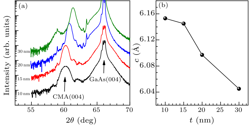
Fig. 2. (a) XRD $\theta$–$2\theta$ scans for CMA films, with $t$ increasing from 2.5 nm to 30 nm. (b) The relation of $c$ versus $t$.
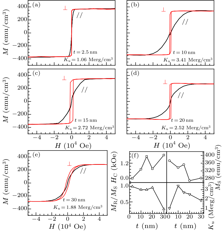
The CMA (004) peak is shown in Fig. 2(a) in more detail, where it shifts to a higher angle with increasing $t$. According to Bragg's law $2d\sin\theta=n\lambda$, where $d$ is the spacing of the crystal planes, $\theta$ is the angle between the x-ray and the corresponding crystal plane, $n$ is an integer, $\lambda$ is the wavelength of the x-ray used, and $\theta$ shifts to a higher angle when the spacing of the (001) crystal planes decreases. Except for the 2.5-nm-thick sample with weak diffraction signal (unplotted), no other significant XRD peaks are observed among the other films, indicating that the ${c}$-axis remains normal to the sample surface. As shown in Fig. 2(b), the lattice constant $c$ decreases from 6.153 Å to 6.045 Å as $t$ increases from 10 nm to 30 nm. Taking into consideration the $a$ value (5.658 Å) of the 2.5-nm-thick sample, the structure of the CMA deviates from that of cubic structures as a result of the compressive strain at the interface between GaAs and CMA. Hence, more crystal cells bear the strain with increasing $t$, which results in the decrease of the deviation of a single crystal cell. Therefore, the $c$ value decreases towards the bulk value when $t$ increases. The magnetic properties of CMA films are shown in Figs. 3(a)–3(f). A magnetic field up to 5 T was applied perpendicularly ($\bot $) or parallel ($\parallel$) to the film plane. In contrast to Co$_{2}$MnAl films, the hysteresis loops with the field applied in the [1-10] and [110] directions are identical. All the tested samples exhibit PMA and soft magnetic behavior with coercive fields less than $2\times 10^{-1}$ T. The saturation magnetization $M_{\rm S}$ related to the crystallization of the material decreases from 370 emu/cm$^{3}$ to 280 emu/cm$^{3}$, indicating the emergence of more defects as strain relaxation. The loop squareness $M_{\rm R}/M_{\rm S}$ decreases rapidly as $t$ reaches 30 nm, as shown in Figs. 3(e) and 3(f). The uniaxial magnetic anisotropy energy $K_{\rm u}$ is determined by the relation $K_{\rm u}=K^{\rm eff}+2\pi M_{\rm S}^{2}$,[15,16] where $K^{\rm eff}$ denotes the magneto-crystalline anisotropy energy, which could be calculated by the area enclosed by the out-of-plane and in-plane magnetization curves, and 2$\pi M_{\rm S}^{2}$ denotes the demagnetization energy originating from shape anisotropy. The value of $K_{\rm u}$ of the CMA layers, comparable to that of conventional PMA materials,[17,18] versus $t$ is also shown in Fig. 3(f). Disregarding the 2.5-nm-thick sample, $K_{\rm u}$ decreases from 3.41 Merg/cm$^{3}$ to 1.88 Merg/cm$^{3}$ as $t$ increases from 10 nm to 30 nm, which could be attributed to the fact that the lattice is transforming to a cubic structure with strain relaxation accompanying the growth of CMA films. The compressive strain denoted by $c/a_{\rm GaAs}$ for the 10-nm-thick film with the maximum $K_{\rm u}$ is calculated to be 1.089. The characteristic values of the magnetic properties of CMA films are listed in Table 1. The value of $K_{\rm u}$ and the effective magnetic anisotropy field of the 2.5-nm-thick sample turn out to be much smaller than those of the other samples, indicating that the PMA of CMA films does not come from the interfacial magnetic anisotropy but is related to a strain-induced bulk effect, different from that of Co$_{2}$FeAl/MgO.[11] To be more accurate, the PMA of CMA films macroscopically originates from the symmetry of their structure deviated from the cubic structure.[19,20] The $K_{\rm u}$ value of the 10-nm-thick CMA film is also comparable with that of perpendicular CoFeB/MgO used in conventional MTJ.[21] In addition, since the PMA of the CMA films is not limited to several nanometers, the magnetic thermal stability of CMA films could be much enhanced with increasing the volume.
Table 1. The characteristic values of the magnetic properties of CMA films, with $t$ increasing from 2.5 nm to 30 nm.
$t$ $c/a_{\rm GaAs}$ $M_{\rm S}$ $H_{\rm C}$ $M_{\rm R}/M_{\rm S}$ $K_{\rm u}$
(nm) (emu/cm$^{3})$ (Oe) (Merg/cm$^{3}$)
2.5 373 $ < 100$ 0.995 1.06
10 1.089 337 730 0.895 3.41
15 1.088 353 1700 0.895 2.72
20 1.079 270 770 0.964 2.52
30 1.070 280 1830 0.265 1.88
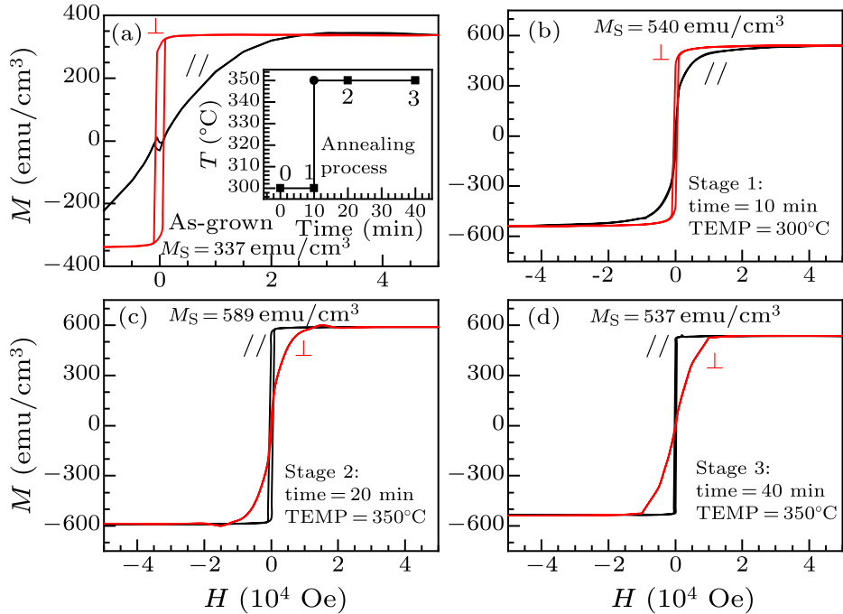
To demonstrate the thermal stability, annealing treatment, which could increase the crystallinity but release the strain in the films, was carried out on the same 10-nm-thick sample. Figure 4(a) shows the hysteresis loop of the as-grown sample. The annealing process is shown in the inset of Fig. 4(a). The hysteresis loops at different annealing stages are shown in Figs. 4(b)–4(d). Stage 1: the sample was annealed at 300$^{\circ}\!$C for 10 min where it still has PMA with $K_{\rm u}=3.38$ Merg/cm$^{3}$. The rapid rise of $M_{\rm S}$ indicates the distinct increase in the crystallization or the short-range order of the film. Stage 2: it was then annealed at 350$^{\circ}\!$C for 10 min. As shown in Fig. 4(c), the easy axis rotates from the out-of-plane to the in-plane after annealing. Stage 3: after another 20 min annealing at 350$^{\circ}\!$C, the loop plotted in Fig. 4(d) is almost the same as that shown in Fig. 4(c), indicating a stable phase, which is likely a strain-free cubic structure for the temperature of 350$^{\circ}\!$C. According to the above analyses, the residual strain in the CMA films is relaxed when the sample is annealed at 350$^{\circ}\!$C. The strain relaxation is possibly caused by an unstable interface resulting from the interfacial reaction between CMA and GaAs, which is commonly observed in Mn-based alloy grown on GaAs substrates.[22,23]
cpl-36-6-067502-fig3.png
Fig. 3. (a)–(e) Hysteresis loops of CMA films with different $t$ values. (f) The change of coercivity ($H_{\rm C}$), saturation magnetization ($M_{\rm S}$), loop squareness ($M_{\rm R}/M_{\rm S}$) and PMA energy ($K_{\rm u}$) versus $t$.
cpl-36-6-067502-fig4.png
Fig. 4. (a) The hysteresis loop of the as-grown 10 nm sample. The inset shows the annealing process on the same 10-nm-thick film. (b)–(d) The hysteresis loops of the films at different annealing stages corresponding to the point in the inset of (a).
In summary, we have investigated the crystalline structure and the magnetic properties of specific off-stoichiometric Heusler alloy Co$_{2}$MnAl films with different thicknesses. The PMA in CMA films can be realized and modulated by the lattice distortion originating from residual compressive strain in the films. It is noted that the PMA can be tuned from 3.41 Merg/cm$^{3}$ to 1.88 Merg/cm$^{3}$ with the thickness changing from 10 nm to 30 nm. Compared to the other perpendicular magnetized Heusler alloy films with the thickness limited to several nanometers, the CMA films show well-squared out-of-plane hysteresis loops with a thickness up to 20 nm. Moreover, the PMA of CMA films is stable after annealing at up to 300$^{\circ}\!$C and vanishes above 350$^{\circ}\!$C. Although the spin polarization of CMA films still remains to be calculated and tested, off-stoichiometric full-Heusler compounds with residual strain may be a kind of magnetic material with PMA and high spin polarization.
References New Class of Materials: Half-Metallic FerromagnetsMagnetic anisotropy, exchange and damping in cobalt-based full-Heusler compounds: an experimental review Co 2 Mn X ( X = Si , Ge, Sn) Heusler compounds: An ab initio study of their structural, electronic, and magnetic properties at zero and elevated pressureSimple rules for the understanding of Heusler compoundsPerpendicular all the wayPerpendicular magnetic tunnel junction and its application in magnetic random access memoryHigh-Power Coherent Microwave Emission from Magnetic Tunnel Junction Nano-oscillators with Perpendicular AnisotropySpin-polarized tunnelingMnGa-based fully perpendicular magnetic tunnel junctions with ultrathin Co2MnSi interlayersFabrication of perpendicularly magnetized magnetic tunnel junctions with L10-CoPt/Co2MnSi hybrid electrodeMagnetic Tunnel Junctions with Perpendicular Anisotropy Using a Co$_{2}$FeAl Full-Heusler AlloyMagnetic and transport properties of Mn 2 CoAl oriented filmsThe effect of Mn content on magnetism and half-metallicity of off-stoichiometric Co 2 MnAlThickness dependence of magnetic anisotropy and intrinsic anomalous Hall effect in epitaxial Co2MnAl filmPerpendicular magnetic properties of ultrathin L10-Mn1.67Ga films grown by molecular-beam epitaxyMultifunctional L10-Mn1.5Ga Films with Ultrahigh Coercivity, Giant Perpendicular Magnetocrystalline Anisotropy and Large Magnetic Energy ProductUltrathin Co/Pt and Co/Pd superlattice films for MgO-based perpendicular magnetic tunnel junctionsTunnel Magnetoresistance Over 100% in MgO-Based Magnetic Tunnel Junction Films With Perpendicular Magnetic L1$_{0}$-FePt ElectrodesPerpendicular Magnetic Anisotropy Induced by Tetragonal Distortion of FeCo Alloy Films Grown on Pd(001)Stoichiometry dependent phase transition in Mn-Co-Ga-based thin films: From cubic in-plane, soft magnetized to tetragonal perpendicular, hard magnetizedA perpendicular-anisotropy CoFeB–MgO magnetic tunnel junctionMagnetic structure of Co 1 x Mn x alloysInterfacial reactions of Mn/GaAs thin films
[1] de Groot R A, Mueller F M, van Engen P G and Buschow K H J 1983 Phys. Rev. Lett. 50 2024
[2] Trudel S, Gaier O, Hamrle J and Hillebrands B 2010 J. Phys. D 43 193001
[3] Picozzi S, Continenza A and Freeman A J 2002 Phys. Rev. B 66 094421
[4] Graf T, Felser C and Parkin S S P 2011 Prog. Solid State Chem. 39 1
[5] Kent A D 2010 Nat. Mater. 9 699
[6] Liu H F, Ali S S and Han X F 2014 Chin. Phys. B 23 077501
[7] Zeng Z, Amiri P K, Krivorotov I N, Zhao H, Finocchio G, Wang J P, Jordan A K, Huai Y M, Langer J, Galatsis K, Wang K L and Jiang H W 2012 ACS Nano 6 6115
[8] Hirohata A, Frost W, Samiepour M and Kim J Y 2018 Materials 11 105
[9] Mao S W, Lu J, Zhao X P, Wang X L, Wei D H, Liu J, Xia J B and Zhao J H 2017 Sci. Rep. 7 43064
[10] Hiratsuka T, Kim G, Sakuraba Y, Kubota T, Kodama K, Inami N, Naganuma H, Oogane M, Nakamura T, Takanashi K and Ando Y 2010 J. Appl. Phys. 107 09C714
[11] Wen Z, Sukegawa H, Kasai S, Hayashi M, Mitani S and Inomata K 2012 Appl. Phys. Express 5 063003
[12] Jamer M E, Assaf B A, Devakul T and Heiman D 2013 Appl. Phys. Lett. 103 142403
[13] Feng Y, Zhou T, Chen X, Yuan H and Chen H 2015 J. Magn. Magn. Mater. 387 118
[14] Meng K K, Miao J, Xu X G, Zhao J H and Jiang Y 2017 Phys. Lett. A 381 1202
[15] Xiao J X, Lu J, Zhu L J and Zhao J H 2016 Acta Phys. Sin. 65 118105 (in Chinese)
[16] Zhu L J, Nie S H, Meng K K, Pan D, Zhao J H and Zheng H 2012 Adv. Mater. 24 4547
[17] Yakushiji K, Saruya T, Kubota H, Fukushima A, Nagahama T, Yuasa S and Ando K 2010 Appl. Phys. Lett. 97 232508
[18] Yoshikawa M, Kitagawa E, Nagase T, Daibou T, Nagamine M, Nishiyama K, Kishi T and Yoda H 2008 IEEE Trans. Magn. 44 2573
[19] Winkelmann A, Przybylski M, Luo F, Shi Y and Barthel J 2006 Phys. Rev. Lett. 96 257205
[20] Ouardi S, Kubota T, Fecher G H, Stinshoff R, Mizukami S, Miyazaki T, Ikenaga E and Felser C 2012 Appl. Phys. Lett. 101 242406
[21] Ikeda S, Miura K, Yamamoto H, Mizunuma K, Gan H D, Endo M, Kanai S, Hayakawa J, Matsukura F and Ohno H 2010 Nat. Mater. 9 721
[22] Wu D, Liu G L, Jing C, Wu Y Z, Loison D, Dong G S, Jin X F and Wang D S 2001 Phys. Rev. B 63 214403
[23] Hilton J L, Schultz B D, McKernan S and Palmstrøm C J 2004 Appl. Phys. Lett. 84 3145