Chinese Physics Letters, 2019, Vol. 36, No. 2, Article code 028401 Ultrafast Carrier Dynamics and Terahertz Photoconductivity of Mixed-Cation and Lead Mixed-Halide Hybrid Perovskites * Wan-Ying Zhao (赵婉莹)1, Zhi-Liang Ku (库治良)2, Li-Ping Lv (吕丽萍)3, Xian Lin (林贤)1, Yong Peng (彭勇)2, Zuan-Ming Jin (金钻明)1,4**, Guo-Hong Ma (马国宏)1,4**, Jian-Quan Yao (姚建铨)5 Affiliations 1Department of Physics, Shanghai University, Shanghai 200444 2State Key Laboratory of Advanced Technology for Materials Synthesis and Processing, Wuhan University of Technology, Wuhan 430070 3Department of Chemical Engineering, School of Environmental and Chemical Engineering, Shanghai University, Shanghai 200444 4STU & SIOM Joint Laboratory for Superintense Lasers and Applications, Shanghai 201210 5College of Precision Instrument and Opto-electronics Engineering, Institute of Laser and Opto-electronics, Tianjin University, Tianjin 300072 Received 5 September 2018, online 22 January 2019 *Supported by the National Natural Science Foundation of China under Grant Nos 11604202, 11674213, 61735010 and 51603119, the Young Eastern Scholar under Grant Nos QD2015020 and QD2016027, the Shanghai Rising-Star Program under Grant No 18QA1401700, the 'Chen Guang' Project under Grant Nos 16CG45 and 16CG46, the Shanghai Municipal Education Commission, and the Shanghai Education Development Foundation.
**Corresponding author. Email: physics_jzm@shu.edu.cn; ghma@staff.shu.edu.cn
Citation Text: Zhao W Y, Ku Z L, Lv L P, Lin X and Peng Y et al 2019 Chin. Phys. Lett. 36 028401    Abstract Using time-dependent terahertz spectroscopy, we investigate the role of mixed-cation and mixed-halide on the ultrafast photoconductivity dynamics of two different methylammonium (MA) lead-iodide perovskite thin films. It is found that the dynamics of conductivity after photoexcitation reveals significant correlation on the microscopy crystalline features of the samples. Our results show that mixed-cation and lead mixed-halide affect the charge carrier dynamics of the lead-iodide perovskites. In the (5-AVA)$_{0.05}$(MA)$_{0.95}$PbI$_{2.95}$Cl$_{0.05}$/spiro thin film, we observe a much weaker saturation trend of the initial photoconductivity with high excitation fluence, which is attributed to the combined effect of sequential charge carrier generation, transfer, cooling and polaron formation. DOI:10.1088/0256-307X/36/2/028401 PACS:84.60.Jt, 78.47.-p, 07.57.Ty © 2019 Chinese Physics Society Article Text In the past few years, hybrid organic-inorganic lead trihalide perovskite (APbX$_{3}$), such as methylammonium lead triiodide (MAPbI$_{3}$), has received an enormous amount of attention for thin film solar cell materials with efficient light absorption.[1,2] Due to strong light absorption and long charge diffusion length, MAPbI$_{3}$ shows superior photovoltaic properties with marked defect tolerance.[3-5] The power conversion efficiency (PCE) of the solar cell based on hybrid organic-inorganic perovskite film has increased from 10% to 23% in the past few years.[2,6-11] In addition, it is reported that the external quantum efficiency of perovskite reaches 20.3%.[12] This represents a substantial step towards the practical application of perovskite LEDs in lighting and display.[12,13] The stability for the reproducible high efficiency is a major concern towards industrialization. Meanwhile, a large body of work has been devoted to understanding 'why' lead halide perovskites own long carrier lifetimes, large carrier diffusion length and high defect-tolerance. Recently, several groups suggest that a reduced coulomb attraction of the carriers due to the formation of large polarons in the hybrid organic-inorganic lead-iodide perovskites can be regarded as a possible mechanism for the large diffusion length of photo-carriers.[14-16] The crystalline of hybrid organic-inorganic lead halide perovskite structure can be viewed as two interpenetrating sublattices, including the organic sublattice CH$_{3}$NH$_{3}^{+}$ and the inorganic Pb halide octahedral PbX$_{3}^{-}$ sublattice. Generally, both the valence and conduction bands related to charge transport are formed by the inorganic PbX$_{3}^{-}$ sublattice. However, the organic CH$_{3}$NH$_{3}^{+}$ sublattice serves as a medium to modulate the electrostatic landscape experienced by the charge carriers, which could lead to charge screening and localization. To understand photo-induced carrier conductivity and its dynamics, it is very important to identify the role of mixed organic cations and mixed halides anions in this organic-inorganic hybrid peroviskite. To date, the best perovskite solar cells were fabricated using mixed organic cations and mixed halides, which behave higher light harvesting capability, longer charge diffusion length and superior photo-stability than the prototypical pervoskite film, MAPbI$_{3}$.[17,18] Recently, Mei et al. fabricated a perovskite solar cell with a mixed-cation perovskite (5-AVA)$_{x}$(MA)$_{1-x}$PbI$_{3}$, where (5-AVA) is the abbreviation of 5-ammoniumvaleric acid. As compared to MAPbI$_{3}$, the (5-AVA)$_{x}$(MA)$_{1-x}$PbI$_{3}$ was characterized to have a longer exciton lifetime and a higher quantum yield for photoinduced charge separation.[19] Pei et al. reported that the PCE and photo-durability in (5-AVA)$_{y}$(MA)$_{1-y}$PbI$_{3-x}$Cl$_{x}$ were higher than that of (5-AVA)$_{x}$(MA)$_{1-x}$PbI$_{3}$.[18] A possible mechanism behind the durability enhancement in (5-AVA)$_{y}$(MA)$_{1-y}$PbI$_{3-x}$Cl$_{x}$ perovskite was attributed to the crystallographic stability and carrier transport length.[20,21] Even though mixed-cation lead mixed-halide perovskites have lower defect concentration and higher stability, the understanding of doping effect on photo-excited carrier dynamics in (5-AVA)$_{y}$(MA)$_{1-y}$PbI$_{3-x}$Cl$_{x}$ is still lacking because most works have focused on material development and device optimization. Ultrafast photoinduced time-dependent terahertz (THz) conductivity spectra offer a contact-free amperemeter with sub-picosecond time resolution, which have been used to access the carrier transport, such as carrier density, carrier momentum scattering time and the dynamics of photoconductivity.[22,23] In this study, we employ time-domain THz spectroscopy to characterize the THz photo-conductivity changes and its dynamics in prototypical, (5-AVA)$^{+}$- and Cl$^{-}$-codoped MAPbI$_{3}$. The initial dynamics of the photoinduced conductivity reveals significant dependence on the mixed-cation and lead mixed-halide. We find an increased THz photoconductivity in Cl$^{-}$ and (5-AVA)$^{+}$ codoped perovskite. In addition, we investigate the influence of mixed-cation and lead mixed-halide in the (5-AVA)$_{y}$(MA)$_{1-y}$PbI$_{3-x}$Cl$_{x} $ on the initial values of the photoconductivity, which is largely attributed to a combined effect of generation, transfer and cooling of hot carriers, and polaron formation.
cpl-36-2-028401-fig1.png
Fig. 1. (a) A schematic of the crystal structure of the two perovskite films: MAPbI/s and (5-AVA)(MA)PbICl/s. (b) Top-view SEM image of two perovskite films. The scale bar is 5 µm. (c) The normalized UV-visible absorption spectra, and (d) the Tauc plots of the two perovskite films, MAPbI/s and (5-AVA)(MA)PbICl/s.
As shown in Fig. 1(a), MAPbI$_{3}$/spiro-OMeTAD (MAPbI/s), and (5-AVA)$_{0.05}$(MA)$_{0.95}$PbI$_{2.95}$Cl$_{0.05}$ /spiro-OMeTAD ((5-AVA)(MA)PbICl/s) perovskite films were deposited on fused silica substrates by 'one-step' spin-coating method.[19] For the MAPbI$_{3}$ sample, MAPbI$_{3}$ precursor solution was firstly prepared by mixing MAI (0.395 g) and PbI$_{2}$ (1.157 g) in DMF (2 mL) at 70$^{\circ}\!$C with stirring for 24 h. Then, the as-prepared precursor solution was spin-coated on the quartz slide at 3000 rpm, followed by drying at 100$^{\circ}\!$C in glove box. The color of the MAPbI$_{3}$ film turned from yellow to dark gradually, suggesting the removing of solvent and the formation of the MAPbI$_{3}$ perovskite multicrystalline film. On this basis, a (5-AVA$_{0.05}$ MA$_{0.95}$)PbI$_{2.95}$Cl$_{0.05}$ sample was prepared by replacing another 5% of the MAI by (5-AVA)I, which was synthesized according to the method reported by in the previous work.[19] In two sample systems, (5-AVA)$_{y}$(MA)$_{1-y}$PbI$_{3-x}$Cl$_{x} $ is used as the light absorber, while spiro-OMeTAD is used as the hole transport layer. Our deposited films have average thicknesses of 400 nm$\pm$100 nm determined with a surface profilometer. Figure 1(b) shows the surface scanning electron microscopy (SEM) images of the two samples. It is seen that the surface of MAPbI/s exhibits an irregular morphology with roughness. Indeed, manipulating the composition of PbI$_{3}^{-}$ by adding Cl$^{-}$ considerably smooth the surface and leads to the stabilization of the perovskite phase with a uniform and dense morphology. Typical ultraviolet-visible optical absorption spectra at room temperature are shown in Fig. 1(c). All the films show roughly the same absorption edge of $\sim$760 nm. As shown in Fig. 1(d), the Tauc plots reveal that the optical bandgap is around 1.61 eV for all the films, which agrees with both the experimentally measured values ranging from 1.57 to 1.63 eV,[24-26] and results from density functional theory (DFT) calculations.[27] The very close bandgap values may be attributed to the low replacement of (MA)$^{+}$ by (5-AVA)$^{+}$, and $I^{-}$ by Cl$^{-} $, as shown in Fig. 1(d). The XRD results in Fig. S1 demonstrate that our peroviskite films have the tetragonal structure at room temperature, which are in agreement with the previous publication.[28]
cpl-36-2-028401-fig2.png
Fig. 2. (a) Schematic of optical-pump THz-probe spectroscopy for transient photo-conductivity measurements. (b) Time-resolved THz photoconductivity measurements of MAPbI/s and (5-AVA)(MA)PbICl/s at room temperature after photo-excitation at 400 nm. (c) Schematic diagram of the energy levels and charge carrier dynamics after photo-excitation in the perovskite/spiro-OMeTAD sample.
Our optical-pump THz-probe spectroscopy (OPTP) spectroscopy was driven by a Ti:sapphire femtosecond amplifier. The amplified fundamental beam centered at 800 nm (120 fs, 1 kHz) is split into two parts. One part of the laser output is used to generate and detect THz radiation by optical rectification and electro-optical sampling with two 1-mm-thick (110)-orientated ZnTe crystals. The other part is frequency doubled with a $\beta$-BaB$_{2}$O$_{4}$ crystal to deliver photo-energy of 3.1 eV (400 nm), which acts as a pump beam, as shown in Fig. 2(a). The photon energy of pump beam (3.1 eV) exceeds the dual valence band structure of all investigated samples. No significant degradation was observed during the experiments. To avoid absorption of THz radiation due to water vapor, the setup was purged with dry nitrogen. A lock-in amplifier and an optical chopper were used to improve the signal-to-noise ratio in our measurements (see the supplementary material for details). All the experiments were performed at room temperature.
cpl-36-2-028401-fig3.png
Fig. 3. (a) Comparison of the rise dynamics of the photoconductivity (normalized to unity) for two samples. The solid lines show the fits obtained from Eq. (1). The Gaussian instrument response function with FWHM of 120 fs is shown in orange. (b) The normalized $-\frac{\Delta T}{T}(\Delta t)$ for samples. The inset shows the normalized $-\frac{\Delta T}{T}(\Delta t)$ of (5-AVA)(MA)PbICl/s upon excitation at 400 nm with pump fluences of 98 and 195 µJ/cm$^{2}$. The black solid lines are multi-exponential fittings.
We plot the photo-induced peak change of the THz electric-field amplitude as a function of pump-probe time delay $-\frac{\Delta T}{T}(\Delta t)$, for MAPbI/s and (5-AVA)(MA)PbICl/s with a selected pump fluence of 98 µJ/cm$^{2}$, respectively. We show that $-\frac{\Delta T}{T}(\Delta t)$ keeps positive in all the samples, indicating the photo-induced absorption (positive photoconductivity) in all the perovskite films. After photo-excitation at 400 nm, $-\frac{\Delta T}{T}(\Delta t)$ exhibits an instantaneous rise and subsequently relaxation with hundreds of ps time scales. Actually, $-\frac{\Delta T}{T}(\Delta t)$ is correlated to the dynamics of real part of the photo-induced conductivity $\Delta \sigma$,[29,30] which will be discussed in the following. We therefore have shown that the photoconductivity increases during the first $\sim$1.5 ps after photoexcitation and then relaxes to a quasi-steady state. It is noted that the THz conductivity dynamics are dramatically different for samples, under the similar optical excitation condition (the excited sheet densities of $N_{\rm ex}=3.2\times10^{17}$ photon/m$^{2}$). Not only the peak value but also the rise and relaxation dynamical response of $-\frac{\Delta T}{T}(\Delta t)$ are observably dependent on the mixed-cation and lead mixed-halide doping, as shown in Fig. 2(b). We find in our data that a small addition of chloride ions (Cl$^{-}$) to the (5-AVA)(MA)PbI results in a significant increase of photo-conductivity performance. The peak value of $-\frac{\Delta T} {T} (\Delta t)$ for (5-AVA)(MA)PbICl/s is larger than that for MAPbI/s. Our findings are indeed in agreement with the observed morphology of two perovskite films. As shown in Fig. 1(b), the (5-AVA)(MA)PbICl/s shows uniform and dense morphology, and the crystalline features have a much longer length scale than that of MAPbI/s. The well-developed crystallites of (5-AVA)(MA)PbICl/s lead to a reduced backscattering, less additional potential corrugations, and increasing average mobilities. This could be a possible reason for the increasing photoconductivity observed in (5-AVA)(MA)PbICl/s. In addition, as mentioned in previous works, when the spiro-OMeTAD is introduced onto the top surface of the perovskite film, the hole injection from (5-AVA)$_{y}$(MA)$_{1-y}$PbI$_{3-x}$Cl$_{x}$ into spiro-OMeTAD occurs as a primary charge separation process at the interface,[31-33] as the blue dashed arrow shown in Fig. 2(c). The THz conductivity of the perovskite sample with spiro-OMeTAD is about 3–5 times smaller than that of the neat MAPbI$_{3}$.[31,33] The hole-injection process completes on the sub-picosecond time scale in MAPbI/s. Therefore, the photoconductivity measured in our sample systems comes mainly from the electrons left in the perovskite (light absorber layer). Certainly, it should be noted that the rise of $-\frac{\Delta T}{T}(\Delta t)$ could also be inevitably affected by the hole transfer at the interface between (5-AVA)$_{y}$(MA)$_{1-y}$PbI$_{3-x}$Cl$_{x} $ and spiro-OMeTAD. THz transmission signal is not sensitive to the neutral exciton and is only affected by the charge carriers. Actually, the rise of photoconductivity is not limited by the generation of free carriers, which has been reported to occur on sub-100 fs timescales. For a bandgap excitation with a photoenergy of 3.1 eV, as shown in Fig. 2(c), the rapid rising of the photoconductivity shows a combined result: (1) the generation of mobile free electrons in the conduction band, (2) the charge carrier cooling (heat transfer to the lattice), which is determined by optical phonon emission, and (3) the formation of polarons (the dressing of carriers with phonons). As shown in Fig. 3(a), to quantify the observed rising of the THz photoconductivity, we employ a phenomenological model in which a rise component with two effective time constants and a mono-exponential decay with a time constant $\tau_{\rm decay}$ are given by[34,35] $$\begin{alignat}{1} -\frac{\Delta T}{T}(\Delta t)=\,&A\times {\rm {\rm Conv}}(e^{-t/\tau_{\rm decay}},\tau_{\rm pulse})\\ &+B\times {\rm Conv}(e^{-t/\tau_{\rm decay}},\tau_{\rm cooling})\\ &+C\times {\rm Conv}(e^{-t/\tau_{\rm decay}},\tau_{\rm polaron}),~~ \tag {1} \end{alignat} $$ where ${\rm Conv}(e^{-t/\tau_{\rm decay}},\tau)$ is the convolution of $e^{-t/\tau_{\rm decay}}$ with a Gaussian pulse $(\tau_{\rm pulse})$, carrier cooling time $(\tau_{\rm cooling})$, and polaron formation time $(\tau_{\rm polaron})$, respectively. The effective rise time is the amplitude-weight average of these three. Recently, Bretschneider et al. reported that the polaron behavior in lead-iodide perovskites originates from the coupling of charge carriers to lead-halide lattice rather than to organic cations.[36] Thus the timescale of polaron formation can be estimated simply from LO phonon oscillation period of 330 fs, which is consistent with their experimental result of about 400 fs.[36] From the fitting within the assumption of $\tau_{\rm polaron} =400$ fs for MAPbI/s, the extracted cooling time $\tau_{\rm cooling}=1.1\pm0.1$ ps are almost the same for two samples. Then, we fix $\tau_{\rm cooling}=1.1$ ps and make $\tau_{\rm polaron}$ as a free fitting parameter for (5-AVA)(MA)PbICl/s. From the fitting, we obtain $\tau_{\rm polaron}=0.45\pm 0.02$ ps, which is around 10% larger than that of MAPbI. As shown in Fig. 3(b), $-\frac{\Delta T}{T}(\Delta t)$ is normalized to unity, which allows us to compare the evolution of the photoconductivity decay dynamics with multi-exponential fits. The previous studies showed that the carrier mobility remains constant for at least $\sim$1 ns.[37,38] As a matter of fact, the photo-carrier dynamics mainly includes three processes: monomolecular charge-recombination, bimolecular electron-hole recombination and the Auger recombination.[38,39] As shown in the inset of Fig. 3(b), the photo-carrier relaxation dynamics of (5-AVA)(MA)PbICl/s become faster under higher pump fluence, which indicates that a second-order recombination process involved.[39] In addition, it is found that the photo-carrier relaxation of MAPbI/s has an initial fast component compared to that of (5-AVA)(MA)PbICl/s under the similar excitation condition. In detail, the multi-exponential fits of the THz photoconductivity signals give a fast delay component of $\tau_{1}\sim50\pm 3$ ps and a slow delay of $\tau_{2}\sim230\pm 3$ ps for the MAPbI/s. In contrast, the photoconductivity decay for (5-AVA)(MA)PbICl/s can be well reproduced with a single exponential function with fitting lifetime of $1223\pm 3$ ps. The fast component ($\tau_{1}\sim50\pm 3$ ps) in MAPbI/s is typically related to the charge trapping by surface states,[40,41] as the orange arrow shown in Fig. 2(c). The disappearance of fast component in the doped perovskite films could be due to the unintentionally passivation by changing the mixed-cation of (5-AVA)(MA), and as a result, a better compactness, close-packed structure (as shown in Fig. 1(b)) is formed, which results in a reduction of surface recombination.
cpl-36-2-028401-fig4.png
Fig. 4. The excitation-fluence-dependent $-\frac{\Delta T}{T}(\Delta t)$ of THz photoconductivity corresponding to time delay of (a) $\Delta t=0$ ps (peak values), (b) $\Delta t=5$ ps, and (c) $\Delta t=10$ ps. The lines are guide for the eyes.
Figure 4 shows the peak amplitude of $-\frac{\Delta T}{T}(\Delta t)$ as a function of pump fluence (incident photo flux) ranging from 98 to 326 µJ/cm$^{2}$, which shows significantly different trends in prototypical MAPbI/s and codoping (5-AVA)(MA)PbICl/s films. We observe a sub-linear pump fluence dependence of $-\frac{\Delta T}{T}(\Delta t=0\,{\rm ps})$ in MAPbI/s, which is consistent with our previous work.[33] However, the initial photoconductivity follows a nearly linear relationship with pump fluence in (5-AVA)(MA)PbICl/s. It can be found that the different trends of $-\frac{\Delta T}{T}(\Delta t=0\,{\rm ps})$ between the MAPbI/s and the (5-AVA)(MA)PbICl/s become increasing larger under higher excitation densities, while the photoconductivities measured at $\Delta t= 5\,{\rm ps}$ and $\Delta t= 10\,{\rm ps}$ have similar excitation fluence dependences, as shown in Figs. 4(b) and 4(c). Therefore, the fluence-dependent initial photoconductivity can be explained by a combined effect of free carriers dissociated by excitons, free carriers transfer and cooling, and also the formation dynamics of a polaron. In detail, on the one hand, a stronger Coulomb screening means the larger dielectric constant and the lower exciton binding energy, which will consequently make it more easier for excitons dissociate into free carriers.[42,43] On the other hand, the polaron formation will result in an increasing effective mass by 20–45%, which could reduce the conductivity consequently.[44] Furthermore, the charge transport is also affected by the electron-phonon coupling constants.[45] Therefore, a laser pulse with shorter pulse width is required to distinguish each contribution of this combined effect, which is presently beyond the capabilities of our experiments.
cpl-36-2-028401-fig5.png
Fig. 5. (a) The transient sheet THz photoconductivity $\Delta \sigma_{\rm 2D}$ of (5-AVA)(MA)PbICl/s. (b) The real and imaginary parts of the photoconductivity spectrum for (5-AVA)(MA)PbICl/s, which are taken at $\Delta t=5$ ps.
Finally, we acquire the dynamics of the real-part sheet photoconductivity $\Delta \sigma_{\rm 2D}$. As shown in Fig. 5(a), $\Delta \sigma_{\rm 2D}$ is reconstructed from $-\frac{\Delta T}{T}(\Delta t)$ using a thin-film approximation known as the Tinkham equation[46,47] $$\begin{alignat}{1} \Delta \sigma_{\rm 2D} (\Delta t)=(1+n)/Z_{0} [1/(1+\Delta T/T)-1],~~ \tag {2} \end{alignat} $$ where $n$ is the refractive index of the material next to the photoexcited layer. In our case, the photoexcited layer is thinner than the sample, thus $n\approx 6$ is the THz refractive index of the perovskite film, as reported by Sendner et al.[45] $Z_{0} =377$ $\Omega$ is the impedance of free space. The magnitude of $\Delta \sigma_{\rm 2D} $ is scaled to the product of the time-dependent carrier density and mobility of the photo-excited charge carriers. Figure 5(b) shows the flat real component of the measured photoconductivity with small negative imaginary component for (5-AVA)(MA)PbICl/s. Although the conductivity spectrum can be described by the Drude–Smith model, the photoconductivity reveals no significant frequency dependence within the 0.5–2 THz frequency window. This indicates that the carrier scattering time of all the samples is less than 20 fs. In summary, we have demonstrated a comparative study of THz photo-conductivities of hybrid organic-inorganic lead halide perovskites. We have also investigated the role of the different doping extrinsic ions on the initial and relaxation dynamics of photoconductivity. The observed picosecond rise in the photoconductivity can be described by a combined effect of the generation, transfer, cooling of hot carriers, and also the formation of a polaron. Combined with the morphology analysis, we find that manipulating the composition of PbI$_{3}^{-}$ by adding Cl$^{-}$ considerably can smooth the surface and can lead to the stabilization of the perovskite phase with compact, uniform and well-developed crystallites, which are important for the highly improved photoconductivity.
References Efficient Hybrid Solar Cells Based on Meso-Superstructured Organometal Halide PerovskitesIntriguing Optoelectronic Properties of Metal Halide PerovskitesEfficient planar heterojunction perovskite solar cells by vapour depositionSpatial and temporal imaging of long-range charge transport in perovskite thin films by ultrafast microscopyLong-Range Balanced Electron- and Hole-Transport Lengths in Organic-Inorganic CH3NH3PbI3Mesoscopic CH 3 NH 3 PbI 3 /TiO 2 Heterojunction Solar CellsCesium-containing triple cation perovskite solar cells: improved stability, reproducibility and high efficiencyA fluorene-terminated hole-transporting material for highly efficient and stable perovskite solar cellsTemperature-assisted rapid nucleation: a facile method to optimize the film morphology for perovskite solar cellsFacile fabrication of perovskite layers with large grains through a solvent exchange approachNew insight into solvent engineering technology from evolution of intermediates via one-step spin-coating approachPerovskite light-emitting diodes with external quantum efficiency exceeding 20 per centEfficient and stable emission of warm-white light from lead-free halide double perovskitesLong-Lived Photoinduced Polarons in Organohalide PerovskitesCharge Carriers in Hybrid Organic–Inorganic Lead Halide Perovskites Might Be Protected as Large PolaronsElectron–Phonon Coupling and Polaron Mobility in Hybrid Perovskites from First PrinciplesA mixed-cation lead mixed-halide perovskite absorber for tandem solar cellsCompositional engineering of perovskite materials for high-performance solar cellsA hole-conductor-free, fully printable mesoscopic perovskite solar cell with high stabilityEffect of Codoping Cl Anion and 5-AVA Cation on Performance of Large-Area Perovskite Solar Cells with Double-Mesoporous LayersElectron-Hole Diffusion Lengths Exceeding 1 Micrometer in an Organometal Trihalide Perovskite AbsorberPhonon–Electron Scattering Limits Free Charge Mobility in Methylammonium Lead Iodide PerovskitesCarrier dynamics in semiconductors studied with time-resolved terahertz spectroscopyChemical Management for Colorful, Efficient, and Stable Inorganic–Organic Hybrid Nanostructured Solar CellsNanocrystalline/microcrystalline materials based on lead-halide unitsAll-solid-state hybrid solar cells based on a new organometal halide perovskite sensitizer and one-dimensional TiO2 nanowire arraysFirst-Principles Modeling of Mixed Halide Organometal Perovskites for Photovoltaic ApplicationsIdentification and characterization of the intermediate phase in hybrid organic–inorganic MAPbI 3 perovskiteExploring Dynamics in the Far-Infrared with Terahertz SpectroscopyA review of the electrical properties of semiconductor nanowires: insights gained from terahertz conductivity spectroscopyOrganometal Halide Perovskite Solar Cell Materials Rationalized: Ultrafast Charge Generation, High and Microsecond-Long Balanced Mobilities, and Slow RecombinationUnravelling the mechanism of photoinduced charge transfer processes in lead iodide perovskite solar cellsUltrafast Terahertz Probes of Charge Transfer and Recombination Pathway of CH 3 NH 3 PbI 3 PerovskitesPhotoexcited terahertz conductivity dynamics of graphene tuned by oxygen-adsorptionCompeting Ultrafast Energy Relaxation Pathways in Photoexcited GrapheneQuantifying Polaron Formation and Charge Carrier Cooling in Lead-Iodide PerovskitesExcited state and charge-carrier dynamics in perovskite solar cell materialsHigh Charge Carrier Mobilities and Lifetimes in Organolead Trihalide PerovskitesHybrid Perovskites for Photovoltaics: Charge-Carrier Recombination, Diffusion, and Radiative EfficienciesUltrafast terahertz probe of photoexcited free charge carriers in organometal CH3NH3PbI3 perovskite thin filmLow surface recombination velocity in solution-grown CH3NH3PbBr3 perovskite single crystalFree Carrier Emergence and Onset of Electron–Phonon Coupling in Methylammonium Lead Halide Perovskite FilmsDirect Observation of Ultrafast Exciton Dissociation in Lead Iodide Perovskite by 2D Electronic SpectroscopyCalculating polaron mobility in halide perovskitesOptical phonons in methylammonium lead halide perovskites and implications for charge transportConductivity of Superconducting Films for Photon Energies between 0.3 and 4 0 k T c Ultrafast Terahertz Photoconductivity of Photovoltaic Polymer–Fullerene Blends: A Comparative Study Correlated with Photovoltaic Device Performance
[1] Lee M M, Teuscher J, Miyasaka T, Murakami T N and Snaith H J 2012 Science 338 643
[2] Manser J S, Christians J A and Kamat P V 2016 Chem. Rev. 116 12956
[3] Liu M, Johnston M B and Snaith H J 2013 Nature 501 395
[4] Guo Z, Manser J S, Wan Y, Kamat P V and Huang L 2015 Nat. Commun. 6 7471
[5] Xing G, Mathews N, Sun S, Lim S S, Lam Y M, Grätzel M, Mhaisalkar S and Sum T C 2013 Science 342 344
[6] Etgar L, Gao P, Xue Z, Peng Q, Chandiran A K, Liu B, Nazeeruddin M K and Grätzel M 2012 J. Am. Chem. Soc. 134 17396
[7] Saliba M, Matsui T, Seo J, Domanski K, Correa-Baena J P, Nazeeruddin M K, Zakeeruddin S M, Tress W, Abate A, Hagfeldt A, and Grätzel M 2016 Energy Environ. Sci. 9 1989
[8] Jeon N J, Na H, Jung E H, Yang T Y, Lee Y G, Kim G, Shin H, Seok S, Lee J and Seo J 2018 Nat. Energy 3 682
[9] Ren Y, Ding X, Wu Y, Ren Y K, Ding X H, Wu Y H, Zhu J, Hayat T, Alsaedi A, Xu Y, Li Z, Yang S and Dai S Y 2017 J. Mater. Chem. A 5 20327
[10] Ren Y, Shi X, Ding X, Zhu J, Hayat T, Alsaedi A, Li Z, Xu X, Yang S and Dai S Y 2018 Inorg. Chem. Front. 5 348
[11] Ren Y, Duan B, Xu Y, Huang Y, Li Z, Hu L, Hu L, Hayat T, Wang X, Zhu J and Dai S 2017 Sci. Chin. Mater. 60 392
[12] Lin K, Xing J, Quan L, de Arquer F P G, Gong X, Lu J, Xie L, Zhao W, Zhang D, Yan C, Li W, Liu X, Lu Y, Kirman J, Sargent E H, Xiong Q and Wei Z 2018 Nature 562 245
[13] Luo J, Wang X, Li S, Liu J, Guo Y, Niu G, Yao L, Fu Y, Gao L, Dong Q, Zhao C, Leng M, Ma F, Liang W, Wang L, Jin S, Han J, Zhang L, Etheridge J, Wang J, Yan Y, Sargent E H and Tang J 2018 Nature 563 541
[14] Ivanovska T, Dionigi C, Mosconi E, De Angelis F, Liscio F, Morandi V and Ruani G 2017 J. Phys. Chem. Lett. 8 3081
[15] Zhu X Y and Podzorov V 2015 J. Phys. Chem. Lett. 6 4758
[16] Motta C and Sanvito S 2018 J. Phys. Chem. C 122 1361
[17] McMeekin D P, Sadoughi G, Rehman W, Eperon G E, Saliba M, Hörantner M T, Haghighirad A, Sakai N, Korte L, Rech B, Johnston M B, Herz L M and Snaith H J 2016 Science 351 151
[18] Jeon N J, Noh J H, Yang W S, Kim Y C, Ryu S, Seo J and Seok S I 2015 Nature 517 476
[19] Mei A, Li X, Liu L, Ku Z, Liu T, Rong Y, Xu M, Hu M, Chen J, Yang Y, Grätzel M and Han H 2014 Science 345 295
[20] Pei Y, Zou X, Guan Y and Teng G 2016 Int. J. Photoenergy 2016 2953592
[21] Stranks S D, Eperon G E, Graneini G, Menelaou C, Alcocer M J P, Leijtens T, Herz L M, Petrozza A and Snaith H J 2013 Science 342 341
[22] Karakus M, Jensen S A, D'Angelo F, Turchinovich D, Bonn M and Canovas E 2015 J. Phys. Chem. Lett. 6 4991
[23] Ulbricht R, Hendry E, Shan J, Heinz T F and Bonn M 2011 Rev. Mod. Phys. 83 543
[24] Noh J H, Im S H, Heo J H, Mandal T N and Seok S I 2013 Nano Lett. 13 1764
[25] Papavassiliou G C, Pagona G, Karousis N, Mousdis G A, Koutselas I and Vassilakopoulou A 2012 J. Mater. Chem. 22 8271
[26] Qiu J, Qiu Y, Yan K, Zhong M, Mu C, Yan H and Yang S 2013 Nanoscale 5 3245
[27] Mosconi E, Amat A, Nazeeruddin M K, Grätzel M and De Angelis F 2013 J. Phys. Chem. C 117 13902
[28] Guo X, McCleese C, Kolodziej C, Samia A C, Zhao Y and Burda C 2016 Dalton Trans. 45 3806
[29] Schmuttenmaer C A 2004 Chem. Rev. 104 1759
[30] Joyce H J, Bol, J L, Davies C L, Baig S A and Johnston M B 2016 Semicond. Sci. Technol. 31 103003
[31] Ponseca Jr C S, Savenije T J, Abdellah M, Zheng K, Yartsev A, Pascher T, Harlang T, Chabera P, Pullerits T, Stepanov A, Wolf J and Sundstrom V 2014 J. Am. Chem. Soc. 136 5189
[32] Marchioro A, Teuscher J, Friedrich D, Kunst M, Krol R, Moehl T, Grätzel M and Moser J 2014 Nat. Photon. 8 250
[33] Yan H J, Ku Z L, Hu X F, Zhao W Y, Zhong M J, Zhu Q B, Lin X, Jin Z M and Ma G H 2018 Chin. Phys. Lett. 35 028401
[34] Zhang Z, Lin T, Xing X, Lin X, Meng X, Cheng Z, Jin Z and Ma G 2017 Appl. Phys. Lett. 110 111108
[35] Jensen S A, Mics Z, Ivanov I, Varol H S, Turchinovich D, Koppens. H L F, Bonn M and Tielrooij K J 2014 Nano Lett. 14 5839
[36] Bretschneider S A, Ivanov I, Wang H I, Miyata K, Zhu X and Bonn M 2018 Adv. Mater. 30 1707312
[37] Ponseca Jr C S, Tian Y, Sundström V and Scheblykin I G 2016 Nanotechnology 27 082001
[38] Wehrenfennig C, Eperon G E, Johnston M B, Snaith H J and Herz L M 2014 Adv. Mater. 26 1584
[39] Johnston M B and Herz L M 2016 Acc. Chem. Res. 49 146
[40] Yan H, An B, Fan Z, Zhu X, Lin X, Jin Z and Ma G 2016 Appl. Phys. A 122 414
[41] Yang Y, Yan Y, Yang M, Choi S, Zhu K, Luther J M and Beard M C 2015 Nat. Commun. 6 7961
[42] Ghosh T, Aharon S, Etgar L and Ruhman S 2017 J. Am. Chem. Soc. 139 18262
[43] Jha A, Duan H G, Tiwari V, Nayak P K, Snaith H J, Thorwart M and Miller R D 2018 ACS Photon. 5 852
[44] Frost J M 2017 Phys. Rev. B 96 195202
[45] Sendner M, Nayak P K, Egger D A, Beck S, Müller C, Epding B, Kowalsky W, Kronik L, Snaith H J, Pucci A and Lovrinčić R 2016 Mater. Horizons 3 613
[46] Glover I I I R E and Tinkham M 1957 Phys. Rev. 108 243
[47] Jin Z, Gehrig D, Dyer-Smith C, Heilweil E J, Laquai F, Bonn M and Turchinovich D 2014 J. Phys. Chem. Lett. 5 3662
Chinese Physics Letters, 2019, Vol. 36, No. 2, Article code 028102Express Letter Formation of Two-Dimensional AgTe Monolayer Atomic Crystal on Ag(111) Substrate * Li Dong (董立)1,2, Aiwei Wang (王爱伟)1,2, En Li (李恩)1,2, Qin Wang (汪琴)1,2, Geng Li (李更)1,2**, Qing Huan (郇庆)1,2, Hong-Jun Gao (高鸿钧)1,2** Affiliations 1Institute of Physics, Chinese Academy of Sciences, Beijing 100190 2University of Chinese Academy of Sciences, Beijing 100190 Received 15 January 2019, online 18 January 2019 *Supported by the National Key Research & Development Projects of China under Grant Nos 2016YFA0202300 and 2018FYA0305800, the National Natural Science Foundation of China under Grant Nos 61390501, 61474141 and 11604373, the Strategic Priority Research Program of Chinese Academy of Sciences under Grant No XDB28000000.
**Corresponding authors. Email: gengli.iop@iphy.ac.cn; hjgao@iphy.ac.cn
Citation Text: Dong L, Wang A W, Li E, Wang Q and Li G et al 2019 Chin. Phys. Lett. 36 028102    Abstract We report on the formation of two-dimensional monolayer AgTe crystal on Ag(111) substrates. The samples are prepared in ultrahigh vacuum by deposition of Te on Ag(111) followed by annealing. Using a scanning tunneling microscope (STM) and low electron energy diffraction (LEED), we investigate the atomic structure of the samples. The STM images and the LEED pattern show that monolayer AgTe crystal is formed on Ag(111). Four kinds of atomic structures of AgTe and Ag(111) are observed: (i) flat honeycomb structure, (ii) bulked honeycomb, (iii) stripe structure, (iv) hexagonal structure. The structural analysis indicates that the formation of the different atomic structures is due to the lattice mismatch and relief of the intrinsic strain in the AgTe layer. Our results provide a simple and convenient method to produce monolayer AgTe atomic crystal on Ag(111) and a template for study of novel physical properties and for future quantum devices. DOI:10.1088/0256-307X/36/2/028102 PACS:81.05.Zx, 68.37.-d, 81.07.-b, 81.15.Ef © 2019 Chinese Physics Society Article Text Since the first exfoliation of graphene in 2004,[1] research on 2D atomic crystals has become a hot and expanding topic.[2-6] A lot of materials including the graphene[7-9] family (e.g., silicene,[10-12] germanene,[13] antimonene,[14,15] stanene[16] and borophene[17]), transition-metal dichalcogenides (TMDs),[18-21] metal carbides[22] and others have been synthesized in the recent 15 years. Among them, the Te-based 2D atomic crystals have received particular interests. For example, monolayer tungsten ditelluride (WTe$_{2}$), a topologically nontrivial insulator, is reported to host superconductivity under gate control.[19] Structural phase transition is achieved in monolayer molybdenum ditelluride (MoTe$_{2}$) by electrostatic doping.[23] Silver telluride, on the other hand, has been less studied. Ag$_{2}$Te nanocrystals have been demonstrated to be a promising candidate for thermoelectric material[24] and infrared detection.[25] Also, $\beta$ -Ag$_{2}$Te is theoretically predicted to be topologically nontrivial[26,27] and an electronic topological transition in Ag$_{2}$Te is observed under high pressure.[28] Although silver telluride film has been experimentally achieved,[29] monolayer silver telluride has not been reported yet. In this Letter, we report the fabrication of monolayer AgTe film on Ag(111) substrate based on molecular beam epitaxy technique. We conducted all the experiments in a homemade ultrahigh vacuum (UHV) STM system with the base pressure better than $1\times10^{-10}$ mbar. The single crystal Ag(111) (roughness $ < $30 nm, orientation accuracy $ < $0.1$^\circ$, MaTeck Company) was prepared in ultrahigh vacuum by repeated cycles of Ar$^{+}$ ion sputtering and subsequent annealing at 770 K until a clean and atomically flat surface was confirmed by STM imaging. The annealing temperature was measured by an infrared radiation thermometer (Mikron PhotriX$^{\rm TM}$ pyrometer, LumaSense Technologies Company). Te was evaporated with a homemade Knudsen cell (K-cell) evaporator, and the annealing temperature is $\sim$720 K. After the sample preparation, we performed the in situ LEED and STM characterization. All the STM images were taken in a constant-current mode with a bias applied to the sample. The scanning temperature was 80 K.
cpl-36-2-028102-fig1.png
Fig. 1. (a) STM image of large-scale AgTe monolayer on Ag(111) substrate. Scanning parameters: $V_{\rm s}=-0.6$ V, $I_{\rm t}=0.2$ nA. (b) LEED pattern of the sample in (a), with a beam energy of 55.4 eV.
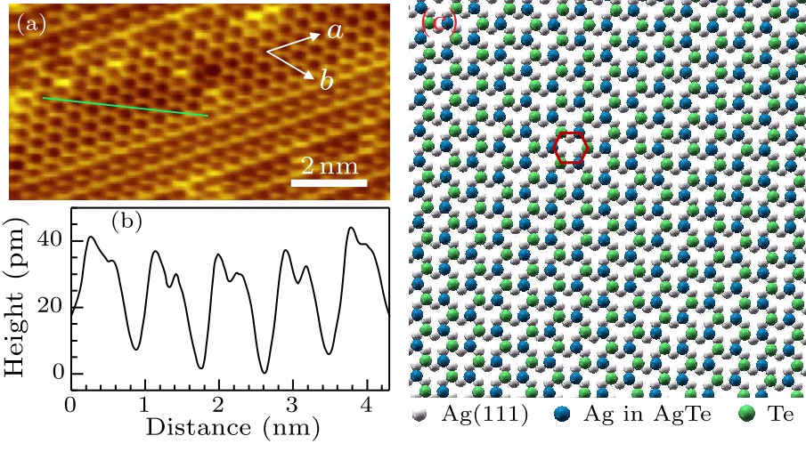
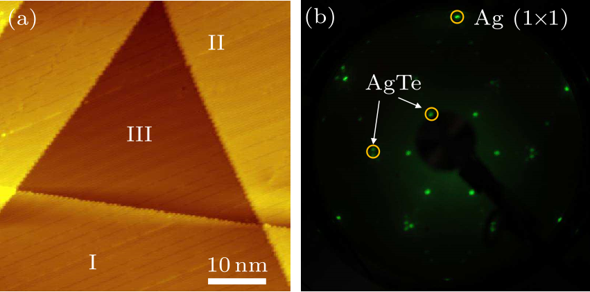
Figure 1(a) shows the large-scale monolayer silver telluride film on Ag(111) substrate. Three different surface regions can be identified. The top and bottom part show features as alternating rows of ridges and trenches, and the middle part shows the periodical stripe-like features. The trench, ridge and stripe regions and labeled by I, II and III, respectively. The LEED image is shown in Fig. 1(b). The outer six spots are attributed to the Ag(111) substrate lattice, and the inner spots are assigned to the AgTe overlayer. Multiple sets of diffraction spots also suggest coexistence of different structures of AgTe monolayer. Figure 2(a) shows the atomic resolution image of the trench regions, and the flat honeycomb structure can be clearly identified. The lattice constants along directions ${\boldsymbol a}$ and ${\boldsymbol b}$ are measured to be 4.85$\pm$0.12 Å and 4.68$\pm$ 0.10 Å, respectively. It should be noted that the piezo of our STM scanner was calibrated by scanning on a standard HOPG substrate. The difference of lattice constants along different high-symmetry directions suggests lattice mismatch between the telluride layer and the substrate as well as the existence of intrinsic in-plane strain in the flat honeycomb area. A line profile is shown in Fig. 2(b), highlighting the cross-sectional information of the topography of the green line in Fig. 2(a). The asymmetry of the two sublattices can be resolved. Based on the above discussions, we speculate that the flat honeycomb area is in fact formed by Ag and Te atoms with 1 to 1 ratio, arranging in a honeycomb manner and each occupying a sublattice. The STM image also rules out the possibility of Ag$_{2}$Te monolayer growth,[27] which would lead to a hexagonal lattice instead of honeycomb. A similar structure was recently proposed on another system, namely CuSe monolayer on Cu(111) substrate.[21] The schematic model in Fig. 2(c) shows ideally the superstructure of the ($1\times 1$) AgTe lattice on a ($\sqrt{3}\times\sqrt{3}$) Ag(111) substrate, with a rotation angle of 30$^\circ$, leading to formation of the flat honeycomb structure.
cpl-36-2-028102-fig2.png
Fig. 2. (a) STM image of monolayer AgTe showing the flat honeycomb regions. Scanning parameters: $V_{\rm s}=-0.6$ V, $I_{\rm t}=0.1$ nA. (b) Line profile of the honeycomb structure showing the asymmetric sublattices. (c) Schematic of the flat honeycomb structure of AgTe on Ag(111) substrate.
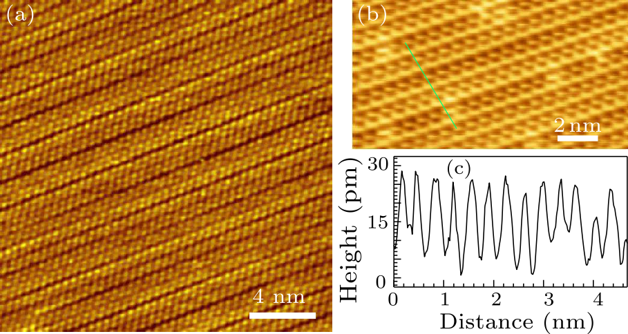
A large-scale STM image for a typical area with the alternating rows of ridges and trenches is shown in Fig. 3(a). Figure 3(b) is a zoom-in image of the "ridge" area. The tilted honeycomb structures appear in double rows, forming the buckled honeycomb area. A height profile is also shown in Fig. 3(c). The origin of the buckled honeycomb structure is not clear yet, and it didn't appear in the Cu–Se system.[20,21] Since we have mentioned the existence of intrinsic in-plane strain in the flat honeycomb, the buckled structure is likely the result of strain relief process. Another experimental evidence supporting this speculation is that we never find large area (e.g., with width $>$5 nm) of the flat honeycomb structure and that it always co-exists with the buckled honeycomb area (Fig. 3(a)). Therefore, the flat honeycomb should be energetically less stable than the buckled honeycomb and the alternating rows of flat and buckled region relieves the strain at the AgTe-substrate interface.
cpl-36-2-028102-fig3.png
Fig. 3. (a) STM image of the buckled honeycomb regions. Scanning parameters: $V_{\rm s}=-1.5$ V, $I_{\rm t}=0.4$ nA. (b) Zoom-in image of (a) showing the buckled honeycomb structure. Scanning parameters: $V_{\rm s}=-0.6$ V, $I_{\rm t}=0.1$ nA. (c) Line profile of the buckled honeycomb structure.
cpl-36-2-028102-fig4.png
Fig. 4. (a) STM image showing the stripe structure. Scanning parameters: $V_{\rm s}=-1.8$ V, $I_{\rm t}=0.8$ nA. (b) Schematic of the stripe formation of the AgTe on Ag(111) substrate.
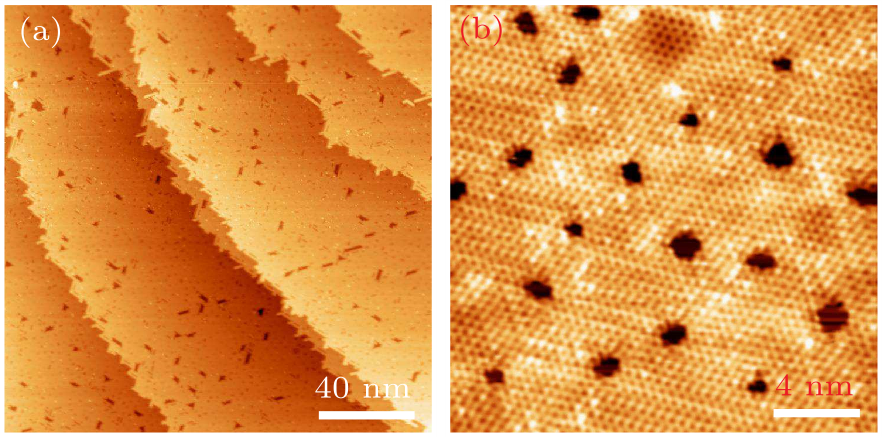
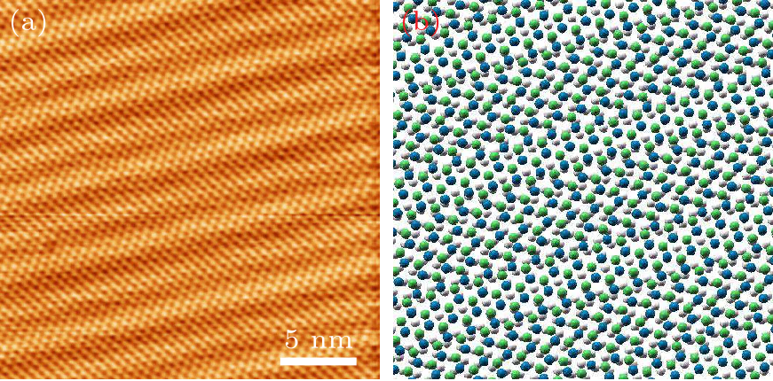
Another way of relieving strain is the formation of stripe structures, as shown in Fig. 4(a). The stripe structure results from the distortion of the honeycomb lattice of the AgTe on Ag(111). Instead of forming the buckled double rows, the honeycomb lattice elongates along the stripe direction, leading to the formation of periodical 1D stripes (1D moiré pattern), as shown in Fig. 4(b). The stripe features give rise to the inner sets of the LEED spots in Fig. 1(b) and the outer sets of spots are caused by the honeycomb structure. We also note that the inner six spots shown in Fig. 1(b) are actually the third-order diffraction spots of the stripe structure, and the first-order spots can only be clearly identified at lower beam energy of such as 25.7 eV. The area of the stripe structure can be much larger ($>$200 nm$\times$200 nm) than the flat honeycomb region, due to a more stable geometry on the surface. Given higher dosage of Te on Ag(111) substrate, the patterned hexagonal structure of the AgTe layer is observed. As shown in Figs. 5(a) and 5(b), the new structure is featured by the emergence of pseudo periodic array of holes, which is similar to another system studied previously.[20] The CuSe grown on Cu(111) substrate also shows that the removal of Cu and Se atoms gives rise to maximum gain of energy and leads to the formation of the ordered array of holes. In our system the holes are also formed since the removal of certain amount of the Ag and Te atoms stabilizes the whole structure. The honeycomb lattice can also be clearly identified in the atomic resolution image in Fig. 5(b). We would also like to note that our ongoing work about Cu$_{2}$Se system suggests no hole formation. The emergence of holes and the honeycomb lattice also support the formation of AgTe. Meanwhile, the distortion of the lattice can also be seen, giving rise to the formation of some triangular shaped regions. The formation of holes and the distortion of the lattice is also closely related to the strain in the AgTe film.
cpl-36-2-028102-fig5.png
Fig. 5. (a) Large-scale and (b) atomic resolution STM images of the AgTe on Ag(111) with higher Te coverage, showing the patterned hexagonal structure of AgTe. Scanning parameters: $V_{\rm s}=-1.8$ V, $I_{\rm t}=0.8$ nA.
In conclusion, we have succeeded in preparation of two-dimensional monolayer AgTe crystal on Ag(111) substrate. The STM and LEED results show that there are four kinds of atomic structures of the samples, which are due to the lattice mismatch, in-plane strain, the atomic interaction at the interface, and the two crystalline orientations. It would be interesting to further investigate the electronic structures of different surface areas of AgTe and also the boundaries between the regions. Further studies of the Ag–Te system on Ag(111) including manipulation of structure and physical property using different techniques are under the way. The fabrication of the novel two-dimensional monolayer AgTe crystal and its technique may pave the way to studying the novel physical properties and practical applications in future topological quantum devices.
References Electric Field Effect in Atomically Thin Carbon Films2D materials and van der Waals heterostructuresConstruction of 2D Atomic Crystals on Transition Metal Surfaces: Graphene, Silicene, and HafneneSponsored Collection | Humble Beginning, Bright Future: Institute of Physics (CAS) at 90Epitaxial growth and physical properties of 2D materials beyond graphene: from monatomic materials to binary compoundsRecent progress in 2D group-VA semiconductors: from theory to experimentFormation of graphene on Ru(0001) surfaceHighly Ordered, Millimeter-Scale, Continuous, Single-Crystalline Graphene Monolayer Formed on Ru (0001)Intercalation of metals and silicon at the interface of epitaxial graphene and its substratesBuckled Silicene Formation on Ir(111)Sequence of Silicon Monolayer Structures Grown on a Ru Surface: from a Herringbone Structure to SiliceneStable Silicene in Graphene/Silicene Van der Waals HeterostructuresBuckled Germanene Formation on Pt(111)Epitaxial Growth and Air-Stability of Monolayer Antimonene on PdTe 2Epitaxial Growth of Flat Antimonene Monolayer: A New Honeycomb Analogue of GrapheneEpitaxial growth of two-dimensional staneneTwo-dimensional boron: structures, properties and applicationsElectronics and optoelectronics of two-dimensional transition metal dichalcogenidesElectrically tunable low-density superconductivity in a monolayer topological insulatorIntrinsically patterned two-dimensional materials for selective adsorption of molecules and nanoclustersEpitaxial Growth of Honeycomb Monolayer CuSe with Dirac Nodal Line Fermions2D metal carbides and nitrides (MXenes) for energy storageStructural phase transition in monolayer MoTe2 driven by electrostatic dopingHeterostructured Approaches to Efficient Thermoelectric MaterialsNear-Infrared Quantum Dots and Their Delicate Synthesis, Challenging Characterization, and Exciting Potential ApplicationsTopological Aspect and Quantum Magnetoresistance of β Ag 2 Te Two-dimensional topological insulators in group-11 chalcogenide compounds: M 2 Te ( M = Cu , Ag ) Electronic Topological Transition in Ag2Te at High-pressureFormation of oriented silver telluride on single and polycrystalline Ag films
[1] Novoselov K S, Geim A K, Morozov S V, Jiang D, Zhang Y, Dubonos S V, Grigorieva I V and Firsov A A 2004 Science 306 666
[2] Novoselov K S, Mishchenko A, Carvalho A and Neto A H C 2016 Science 353 aac9439
[3] Pan Y, Zhang L Z, Huang L, Li L F, Meng L, Gao M, Huan Q, Lin X, Wang Y L, Du S X, Freund H J and Gao H J 2014 Small 10 2215
[4] Zhang G Y, Du S X, Wu K H and Gao H J 2018 Science 360 673
[5] Li G, Zhang Y Y, Guo H, Huang L, Lu H L, Lin X, Wang Y L, Du S X and Gao H J 2018 Chem. Soc. Rev. 47 6073
[6] Zhang S L, Guo S Y, Chen Z F, Wang Y L, Gao H J, Gomez-Herrero J, Ares P, Zamora F, Zhu Z and Zeng H B 2018 Chem. Soc. Rev. 47 982
[7] Pan Y, Shi D X and Gao H J 2007 Chin. Phys. 16 3151
[8] Pan Y, Zhang H G, Shi D X, Sun J T, Du S X, Liu F and Gao H J 2009 Adv. Mater. 21 2777
[9] Huang L, Xu W Y, Que Y D, Mao J H, Meng L, Pan L D, Li G, Wang Y L, Du S X, Liu Y Q and Gao H J 2013 Chin. Phys. B 22 096803
[10] Meng L, Wang Y L, Zhang L Z, Du S X, Wu R T, Li L F, Zhang Y, Li G, Zhou H T, Hofer W A and Gao H J 2013 Nano Lett. 13 685
[11] Huang L, Zhang Y F, Zhang Y Y, Xu W Y, Que Y D, Li E, Pan J B, Wang Y L, Liu Y Q, Du S X, Pantelides S T and Gao H J 2017 Nano Lett. 17 1161
[12] Li G, Zhang L Z, Xu W Y, Pan J B, Song S R, Zhang Y, Zhou H T, Wang Y L, Bao L H, Zhang Y Y, Du S X, Ouyang M, Pantelides S T and Gao H J 2018 Adv. Mater. 30 1804650
[13] Li L F, Lu S Z, Pan J B, Qin Z H, Wang Y Q, Wang Y L, Cao G Y, Du S X and Gao H J 2014 Adv. Mater. 26 4820
[14] Wu X, Shao Y, Liu H, Feng Z, Wang Y L, Sun J T, Liu C, Wang J O, Liu Z L, Zhu S Y, Wang Y Q, Du S X, Shi Y G, Ibrahim K and Gao H J 2017 Adv. Mater. 29 1605407
[15] Shao Y, Liu Z L, Cheng C, Wu X, Liu H, Liu C, Wang J O, Zhu S Y, Wang Y Q, Shi D X, Ibrahim K, Sun J T, Wang Y L and Gao H J 2018 Nano Lett. 18 2133
[16] Zhu F F, Chen W J, Xu Y, Gao C L, Guan D D, Liu C H, Qian D, Zhang S C and Jia J F 2015 Nat. Mater. 14 1020
[17] Zhang Z H, Penev E S and Yakobson B I 2017 Chem. Soc. Rev. 46 6746
[18] Wang Q H, Kalantar-Zadeh K, Kis A, Coleman J N and Strano M S 2012 Nat. Nanotechnol. 7 699
[19] Fatemi V, Wu S F, Cao Y, Bretheau L, Gibson Q D, Watanabe K, Taniguchi T, Cava R J and Jarillo-Herrero P 2018 Science 362 926
[20] Lin X, Lu J C, Shao Y, Zhang Y Y, Wu X, Pan J B, Gao L, Zhu S Y, Qian K, Zhang Y F, Bao D L, Li L F, Wang Y Q, Liu Z L, Sun J T, Lei T, Liu C, Wang J O, Ibrahim K, Leonard D N, Zhou W, Guo H M, Wang Y L, Du S X, Pantelides S T and Gao H J 2017 Nat. Mater. 16 717
[21] Gao L, Sun J T, Lu J C, Li H, Qian K, Zhang S, Zhang Y Y, Qian T, Ding H, Lin X, Du S and Gao H J 2018 Adv. Mater. 30 1707055
[22] Anasori B, Lukatskaya M R and Gogotsi Y 2017 Nat. Rev. Mater. 2 16098
[23] Wang Y, Xiao J, Zhu H Y, Li Y, Alsaid Y, Fong K Y, Zhou Y, Wang S Q, Shi W, Wang Y, Zettl A, Reed E J and Zhang X 2017 Nature 550 487
[24] Zhang Y C and Stucky G D 2014 Chem. Mater. 26 837
[25] van Veggel F C J M 2014 Chem. Mater. 26 111
[26] Zhang W, Yu R, Feng W X, Yao Y G, Weng H M, Dai X and Fang Z 2011 Phys. Rev. Lett. 106 156808
[27] Ma Y D, Kou L Z, Dai Y and Heine T 2016 Phys. Rev. B 93 235451
[28] Zhang Y H, Li Y, Ma Y M, Li Y W, Li G H, Shao X C, Wang H, Cui T, Wang X and Zhu P W 2015 Sci. Rep. 5 14681
[29] Sáfrán G, Geszti O, Radnóczi G 2003 Vacuum 71 299