Chinese Physics Letters, 2017, Vol. 34, No. 4, Article code 048201 Research of Trap and Electron Density Distributions in the Interface of Polyimide/Al$_{2}$O$_{3}$ Nanocomposite Films Based on IDC and SAXS * Yuan-Yuan Liu(刘媛媛)1,2, Jing-Hua Yin(殷景华)1**, Xiao-Xu Liu(刘晓旭)1, Duo Sun(孙夺)1, Ming-Hua Chen(陈明华)1, Zhong-Hua Wu(吴忠华)3, Bo Su(苏玻)1 Affiliations 1Key Laboratory of Engineering Dielectric and Its Applications (Ministry of Education), Harbin University of Science and Technology, Harbin 150080 2Harbin Cambridge College, Harbin 150069 3Institute of High Energy Physics, Chinese Academy of Sciences, Beijing 100049 Received 3 November 2016 *Supported by the National Natural Science Foundation of China under Grant Nos 51337002, 51077028, 51502063 and 51307046, and the Foundation of Harbin Science and Technology Bureau of Heilongjiang Province under Grant No RC2014QN017034.
**Corresponding author. Email: Yinjinghua1@126.com
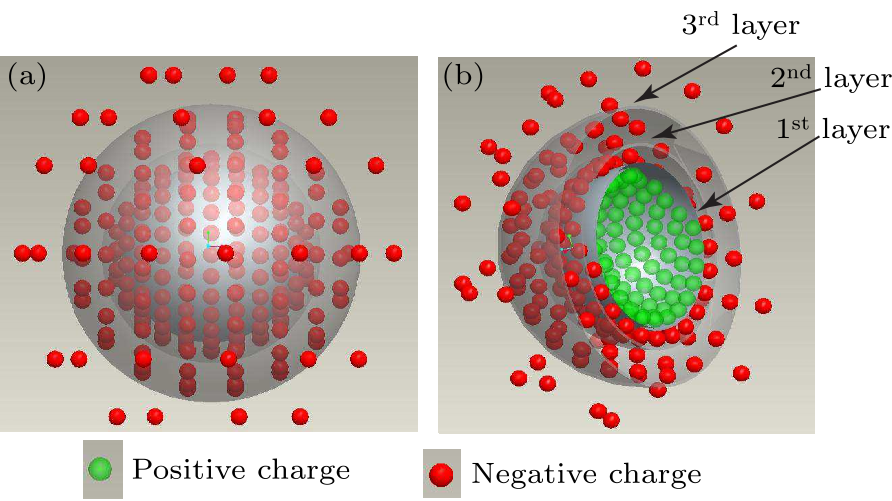
Citation Text: Liu Y Y, Yin J H, Liu X X, Sun D and Chen M H et al 2017 Chin. Phys. Lett. 34 048201 Abstract The distributions of traps and electron density in the interfaces between polyimide (PI) matrix and Al$_{2}$O$_{3}$ nanoparticles are researched using the isothermal decay current and the small-angle x-ray scattering (SAXS) tests. According to the electron density distribution for quasi two-phase mixture doped by spherical nanoparticles, the electron densities in the interfaces of PI/Al$_{2}$O$_{3}$ nanocomposite films are evaluated. The trap level density and carrier mobility in the interface are studied. The experimental results show that the distribution and the change rate of the electron density in the three layers of interface are different, indicating different trap distributions in the interface layers. There is a maximum trap level density in the second layer, where the maximum trap level density for the nanocomposite film doped by 25 wt% is $1.054\times10^{22}$ eV$\cdot$m$^{-3}$ at 1.324 eV, resulting in the carrier mobility reducing. In addition, both the thickness and the electron density of the nanocomposite film interface increase with the addition of the doped Al$_{2}$O$_{3}$ contents. Through the study on the trap level distribution in the interface, it is possible to further analyze the insulation mechanism and to improve the performance of nano-dielectric materials. DOI:10.1088/0256-307X/34/4/048201 PACS:82.35.Np, 82.35.Gh, 68.35.Ct © 2017 Chinese Physics Society Article Text Polymer matrix nanocomposites with numerous superior properties have attracted much attention and have been widely applied in many different fields such as insulation materials, frequency conversion motor and electronic devices.[1-4] The trap effects on electric characteristics have received a great deal of attention due to their unique properties through combination of the properties for organic component.[5] Lei et al. adopted the isothermal decay current (IDC) method to directly measure the trap level density of the Dupont 100CR nanocomposite film and the original polyimide 100HN film, which shows that the trap level density of 100CR is more than twice of 100HN.[6,7] Lewis pointed out that plenty of complex interfaces and traps are formed between polymer and inorganic nanoparticles, where the interface structure of composite films is different from the polymer matrix.[8] Liu et al. also proposed the multi-fractal nanostructures of polyimide films based on SAXS tests.[9] The traps in the interface of polymers can influence the distribution and transport of space charges in nano-dielectrics. The distribution of electron density in the interface of polymers is closely related to space charge distribution, which can reflect the characteristics of trap distribution and carrier transport. To the best of our knowledge, the understanding of the distribution of electron density in the interface of polymers is critical to improve the electrical properties of polymers. In this Letter, we report the study on the electron densities in the interface of PI/Al$_{2}$O$_{3}$ nanocomposite films prepared by the in situ polymerization method, based on the theory of electron density distribution for quasi two-phase mixture doped with spherical nanoparticles. On the basis of the Tanaka multi-core model,[10] the studies on the trap distribution and carrier mobility in the three interface layers were carried out by IDC and SAXS tests, which are also adapted to other nano-dielectrics doped with spherical nanoparticles. Based on the variations of outer circuit current and injected charges, the relationship of carrier mobility $\mu$ and time $t$ can be obtained. When the circuit is shorted, the short circuit current density $J(t)$ can be expressed as[11] $$\begin{align} J(t)=\mu \rho E=\mu El^{-1}\int_0^t {J(\tau)d\tau},~~ \tag {1} \end{align} $$ where $\mu$ is the carrier mobility, $\rho$ is the injected charge density, $E$ is the electric field strength, and $l$ is the depth of the injected charges. According to Poisson's equation, the carrier mobility can be given as follows:[12] $$\begin{align} \mu _{\rm t} =\frac{J(t)\varepsilon l}{[\int\nolimits_0^t {J(\tau)d\tau ]^2}},~~ \tag {2} \end{align} $$ where $\varepsilon$ is the permittivity of PI/Al$_{2}$O$_{3}$ nanocomposite films doped by Al$_{2}$O$_{3}$ (with density of 3.9 g/cm$^{3}$) contents of 5 wt%, 10 wt%, 15 wt%, 20 wt% and 25 wt% in the PI matrix (with density of 1.42 g/cm$^{3}$), and the calculated values are $4.01\times 10^{-12}$, $4.03\times 10^{-12}$, $4.04\times 10^{-12}$, $4.06\times 10^{-12}$ and $4.08\times 10^{-12}$ F/m, based on the Maxwell–Garnett equation.[13] The sample is shorted when $E=0$, the carriers in the low traps are released first, and then the carriers in the deep traps are released. At room temperature, the short circuit current caused by the carriers released with decay time $t$ represents the trap level distribution of the sample surface. Supposing that the carriers released cannot be trapped again, the trap level $E_{\rm t}$ and the current density $J(t)$ can be expressed as[14] $$\begin{align} E_{\rm t}=\,&kT\ln (\nu t),~~ \tag {3} \end{align} $$ $$\begin{align} J(t)=\,&\frac{edkT}{2t}f_0 (E_{\rm t})N(E_{\rm t}),~~ \tag {4} \end{align} $$ where $k$ is the Boltzmann constant, the escape frequency $\nu$ of electrons is $3\times10^{12}$ s$^{-1}$,[15] $T$ is the test temperature, $d$ is the thickness of the sample, $e$ is the electronic charge, $N(E_{\rm t})$ is the trap level density, $f_0 (E_{\rm t})$ in accordance with the Fermi–Dirac distribution function is the probability of energy level $E_{\rm t}$ occupied originally by electrons, and $f_0 (E_{\rm t})=1/2$. The electron density distribution for quasi two-phase mixture doped by spherical inorganic nanoparticles can be given as $$\begin{align} \rho _{\rm c} (r)=\rho (r)\times h(r),~~ \tag {5} \end{align} $$ where $r$ is the scattering vector from the center of the nanoparticle, $\rho _{\rm c} (r)$ is the electron density for quasi two-phase mixture doped by nanoparticles, $\rho (r)$ is the electron density distribution for the ideal two-phase mixture, $h(r)$ is a smooth function associated with the electron density distribution in the interface of quasi two-phase mixture, and it can be expressed as $$\begin{align} h(r)=(2\pi)^{-\frac{3}{2}}\sigma ^{-3}\exp \Big(-\frac{r^2}{2\sigma ^2}\Big).~~ \tag {6} \end{align} $$ The electron density $\rho (r)$ of a nanoparticle is given as $$ \rho (r)=\begin{cases} \!\! \rho _0,&0\leq r\leq R,\\\!\! 0, &r>R, \end{cases}~~ \tag {7} $$ where $R$ and $\rho _0$ are the radius and the electron density of a nanoparticle, respectively. In a polar coordinate system, the electron density $\rho _{\rm c} (r)$ of quasi two-phase mixture can be expressed as $$\begin{align} \rho _{\rm c} (r)=\int {\rho (y)h(r-y)y^2} \sin \alpha d\alpha d\beta dy,~~ \tag {8} \end{align} $$ where $\rho (y)$ and $h(r-y)$ represent the electron density distributions at $y$ and $r-y$ having the properties of spherically symmetric function. Here $\rho _{\rm c} (r)$ can be derived further into $$\begin{align} \rho _{\rm c} (r)=\,&\frac{\rho _0}{\sqrt {2\pi} \sigma r}\int_0^R y\Big[\exp \Big(-\frac{(r-y)^2}{2\sigma ^2}\Big)\\ &-\exp \Big(-\frac{(r+y)^2}{2\sigma ^2}\Big)\Big] dy,~~ \tag {9} \end{align} $$ where $r$ is the radius from the center of nanoparticle, $\sigma$ is a parameter of the interface thickness $D$ calculated according to Porod's Law. Figures 1(a) and 1(b) depict the electron density distribution models of sphere and cross-section views for quasi two-phase mixture, where the fixed layer, the semi-fixed layer and the movable layer in the interface are referred to as the 1st, 2nd and 3rd layers, respectively. The electron density distributions in the three layers of interface are different, where the electron density decreases along the $r$-direction.
cpl-34-4-048201-fig1.png
Fig. 1. The electron density distribution models for quasi two-phase mixture: (a) spherical model and (b) cross-section model.
cpl-34-4-048201-fig2.png
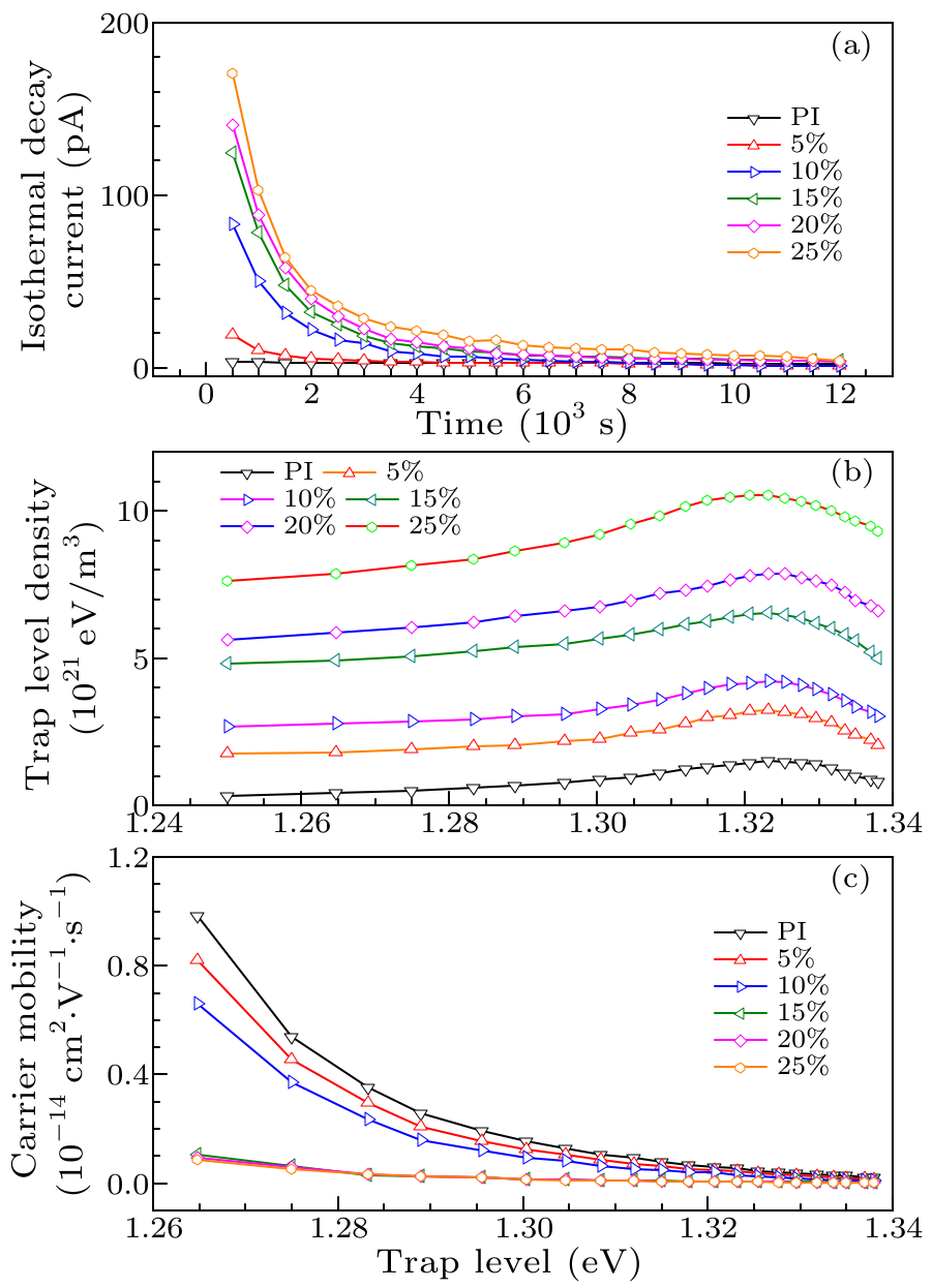
Fig. 2. The characteristic curves of three kinds of nanocomposite films: (a) isothermal decay current $I$ versus time $t$, (b) trap level distributions $N(E_{\rm t})$–$E_{\rm t}$, and (c) $u_{\rm t}$–$E_{\rm t}$.
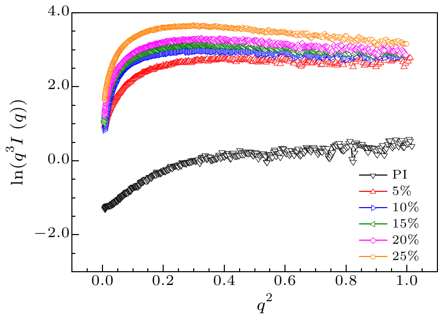
The PI/Al$_{2}$O$_{3}$ nanocomposite films doped by Al$_{2}$O$_{3}$ contents of 5 wt%, 10 wt%, 15 wt%, 20 wt% and 25 wt% were prepared by the in-situ polymerization method. Figure 2(a) gives the characteristic curves of isothermal decay $I$–$t$ for the pure PI and PI/Al$_{2}$O$_{3}$ films at a direct current (DC) electric field of 30 kV/mm. As seen in Fig. 2(a), the IDC change of pure PI with the decay time $t$ in the range of 0–12000 s is not obvious. The IDC of PI/Al$_{2}$O$_{3}$ nanocomposite films, on the other hand, decreases quickly with $t$ in the same time range, and the IDC change increases with the doping contents. Figure 2(b) shows the curves of the trap level density and the trap level of PI/Al$_{2}$O$_{3}$ films doped by different contents. It is clearly seen that the trap level density in the energy range of 1.24–1.34 eV increases when the doping increases,[16] and the maximum trap level density of the film doped by 25 wt% is $1.054\times10^{22}$ eV$\cdot$m$^{-3}$ at 1.324 eV. From Eqs. (2)-(4), the relationship curves of the carrier mobility and the trap level in the nanocomposite films are shown in Fig. 2(c). As seen in Fig. 2(c), the carrier mobility ranges from 0 to $1.0\times10^{-14}$ cm$^{2}$/(V$\cdot$s) and decreases with not only the doped Al$_{2}$O$_{3}$ contents but also the trap level. The reason is that there are a large number of traps in the interface region introduced by doping, and the average distance of free electrons to be trapped is reduced, resulting in a significant decrease of the carrier mobility.[17] The distribution of electron density in the interface is associated with the trap level and the trap level density that can be evaluated by the SAXS test. The Porod plots (${\rm ln}[q^{3}I(q)]$–$q^{2}$) of the PI/Al$_{2}$O$_{3}$ nanocomposite films in the SAXS test are shown in Fig. 3 (where $q$ is the scattering vector, and $I(q)$ is the scattering strength).[18]
cpl-34-4-048201-fig3.png
Fig. 3. The Porod test ${\rm ln}[q^{3}I(q)]$ of the PI/Al$_{2}$O$_{3}$ nanocomposite films versus $q^{2}$.
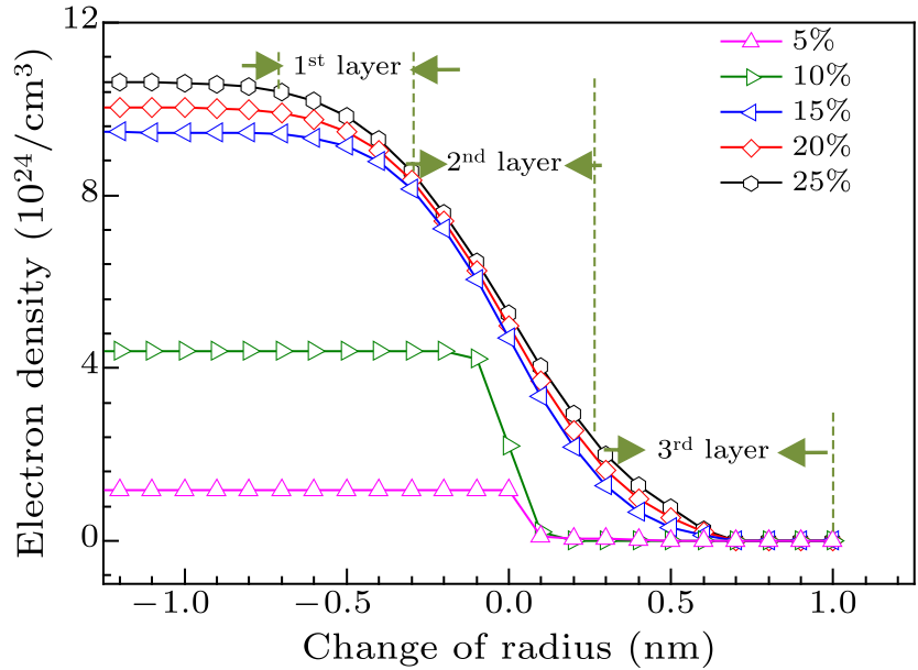
As shown in Fig. 3, the slopes $\sigma$ of the Porod plots gradually change from positive to negative with the addition of doped contents when $q^{2}$ ranges in 0.3–1.0, indicating that there are multi-fractal interfaces formed between the Al$_{2}$O$_{3}$ nanoparticles and the PI matrix. According to Porod's Law, when the Porod plot has a negative slope, the interface thickness $D$ is relative to the slope $\sigma$ of the Porod curve (where $D=\sqrt {2\pi \sigma}$) and can be calculated as listed in Table 1. As listed in Table 1, $D$ increases with the addition of doped Al$_{2}$O$_{3}$ contents, showing that the interaction between PI matrix and nanoparticles is enhanced and the action for binding and anchorage of nanoparticles is improved as well. According to the electron density distribution $\rho _{\rm c} (r)$ of spherical nanoparticle for quasi two-phase mixture, there is an interface with thickness $D$ to be formed between the PI matrix and nanoparticles. From Eq. (9), Fig. 4 shows the distribution curves of electron density of the films related to the distance $\Delta R$ from the radius $R$ position (where the zero point on the horizontal axis is the position of the distance $R$ from the nanoparticle center).
Table 1. Interface thicknesses $D$ of PI/Al$_{2}$O$_{3}$ nanocomposite films doped with different contents.
Contents (wt%) 5 10 15 20 25
$D$ (nm) 0.54 0.61 1.31 1.40 1.48
cpl-34-4-048201-fig4.png
Fig. 4. The electron density distributions in the interface of nanocomposite films.
As shown in Fig. 4, taking the PI/Al$_{2}$O$_{3}$ nano-composite film doped with content of 25 wt% as an example, the interface can be divided into three layers corresponding to the above spherical model. Both the trapped electron density and interface thickness increase with the addition of doped Al$_{2}$O$_{3}$ contents. It is shown that a transition region for the change rate of electrons density occurs around the radius $R$. The change rate of electrons density in the first layer increases along $r$ direction, and it is an approximate maximum in the second layer closed to the radius $R$, after that it decreases in the third layer slowly, corresponding to the changes of trap level density and carrier mobility in the interface. According to the Tanaka multi-core model, the different change rates of electron density along the $r$-direction indicate that the trap level distributions are also different in the three layers. The first layer is formed via close links for ion bonds and covalent bonds between PI and Al$_{2}$O$_{3}$ nanoparticles, where the segments of PI molecular chains are fixed on the surfaces of Al$_{2}$O$_{3}$ nanoparticles. It is the reason for the absence of movable mobility and the high trap level density to occur responding to the high electron density distribution. Through winding between polymer chain segments, the chain segments in the second layer has a certain degree of crystallinity via the binding of fixed layer, thus the change rate of electron density is the most significant compared with the other layers, resulting in the forming of the maximum trap level density and the lowest carrier mobility in this region. The structure of the third layer region being close to the PI matrix is similar to the PI matrix having a small amount of traps, with reduced change rate of the electron density and improved carrier mobility in this region. In conclusion, the maximum trap level density and interface thickness for the nanocomposite film doped with Al$_{2}$O$_{3}$ of 25 wt% are $1.054\times10^{22}$ eV$\cdot$m$^{-3}$ at 1.324 eV and 1.48 nm, respectively, and both of them increase with the addition of doped Al$_{2}$O$_{3}$ contents. The change rate of electron density in the interface is modeled with three layers and the change rates in the three layers are different, thus the trap distributions in the three layers are also different. The maximum trap level density is in the second layer of the interface corresponding to the highest change rate of electron density, resulting in the lowest carrier mobility. The study on the distributions of traps and electron density in the interface of polymers helps to provide the guide for obtaining a higher electrical performance of nano-dielectrics.
References Effect of processing conditions on morphology and mechanical properties of compatibilized polypropylene nanocompositesThermal, mechanical and tribological properties of polyamide 6 matrix composites containing different carbon nanofillersProperties of polyimide/Al2O3 and Si3N4 deposited thin filmsPreparation and characterization of polyimide/Al2O3 hybrid films by sol–gel processInfluence of interface on the electrical properties of polyimide/TiO 2 composite filmsEffect of deep trapping states on space charge suppression in polyethylene/ZnO nanocompositeConduction Current Characteristics and Carrier Mobility of Both Original and Corona-Resistant Polyimide FilmsInterfaces: nanometric dielectricsSmall-Angle X-Ray Scattering Study on Nanostructures of Polyimide FilmsProposal of a multi-core model for polymer nanocomposite dielectricsA space-charge based method for the estimation of apparent mobility and trap depth as markers for insulation degradation-theoretical basis and experimental validationELECTRIC PROPERTIES OF MACROMOLECULES. V. THEORY OF IONIC POLARIZATION IN POLYELECTROLYTESDielectric investigation of thermally-induced chromophore degradation in nonlinear optical polymer electretsSurface charge accumulation and decay on directfluorinated polyimide/Al2O3 nanocompositesSmall-angle X-ray analysis of the effect of grain size on the thermal damage of octahydro-1, 3, 5, 7-tetranitro-1, 3, 5, 7 tetrazocine-based plastic-bounded expolsives
[1] Modesti M, Lorenzetti A, Bon D and Besco S 2005 Polymer 46 10237
[2] Khun N W, Loong P Y, Liu E J and Li L 2015 J. Polym. Eng. 35 23
[3] Tsai M H, Wang H Y, Lu H T, Tseng I H, Lu H H, Huang S L and Yeh J M 2011 Thin Solid Films 519 4969
[4] Ma P C, Nie W, Yang Z H, Zhang P H, Li G, Lei Q Q, Gao L X, Ji X L and Ding M X 2008 J. Appl. Polym. Sci. 108 705
[5] Feng Y, Yin J H, Chen M H and Lei Q Q 2014 IEEE Trans. Dielectr. Electr. Insul. 21 1501
[6] Tian F Q, Lei Q Q, Wang X and Wang Y 2011 Appl. Phys. Lett. 99 142903
[7] Zhang P H, Fan, Y, Wang, F C, Xie H, Li G and Lei Q Q 2005 Chin. Phys. Lett. 22 1253
[8] Lewis T J 2005 J. Phys. D 38 202
[9] Liu X X and Yin J H 2010 Chin. Phys. Lett. 27 096103
[10] Tanaka T, Kozako M, Fuse N and Ohki Y 2005 IEEE Trans. Dielectr. Electr. Insul. 12 669
[11] Mazzanti G, Montanari G C and Alison J M 2003 IEEE Trans. Dielectr. Electr. Insul. 10 187
[12]Alison J M, Mazzanti G, Montanari G C and Palmieri F 2002 Annu. Report Conf. Electr. Insulation Dielectric Phenom. (Cancun Mexico 20–24 October 2002) p 35
[13] O' Konski C T 1960 J. Phys. Chem. 64 605
[14] Watson P K 1998 IEEE Trans. Dielectr. Electr. Insul. 5 21
[15]Wang X, Chen S Q, Cheng X and Tu D M 2009 Proc. CSEE 29 128
[16]Tanaka T 2006 IEEE Conf. Electr. Insulation Dielectric Phenom. (Kansas USA 15–18 October 2006) p 298
[17] Du B X, Li J and Du W IEEE Trans. Dielectr. Electr. Insul. 20 1764
[18] Yan G Y, Tian Q, Lui J H Chen B, Sun G A, Huang M and Li X H 2014 Chin. Phys. B 23 076101