Chinese Physics Letters, 2021, Vol. 38, No. 5, Article code 057304 Transforming a Two-Dimensional Layered Insulator into a Semiconductor or a Highly Conductive Metal through Transition Metal Ion Intercalation Xiu Yan (严秀)1,2, Wei-Li Zhen (甄伟立)1, Shi-Rui Weng (翁士瑞)1, Ran-Ran Zhang (张冉冉)1, Wen-Ka Zhu (朱文卡)1*, Li Pi (皮雳)1,2*, and Chang-Jin Zhang (张昌锦)1,3* Affiliations 1High Magnetic Field Laboratory, Hefei Institutes of Physical Science, Chinese Academy of Sciences, Hefei 230031, China 2University of Science and Technology of China, Hefei 230026, China 3Institutes of Physical Science and Information Technology, Anhui University, Hefei 230601, China Received 5 February 2021; accepted 10 March 2021; published online 2 May 2021 Supported by the National Key Research and Development Program of China (Grant Nos. 2017YFA0403600 and 2016YFA0300404), the National Natural Science Foundation of China (Grant Nos. 11874363, 11974356 and U1932216), and the Collaborative Innovation Program of Hefei Science Center, CAS (Grant No. 2019HSC-CIP002).
*Corresponding authors. Email: wkzhu@hmfl.ac.cn; pili@ustc.edu.cn; zhangcj@hmfl.ac.cn
Citation Text: Yan X, Zhen W L, Weng S R, Zhang R R, and Zhu W K et al. 2021 Chin. Phys. Lett. 38 057304    Abstract Atomically thin two-dimensional (2D) materials are the building bricks for next-generation electronics and optoelectronics, which demand plentiful functional properties in mechanics, transport, magnetism and photoresponse. For electronic devices, not only metals and high-performance semiconductors but also insulators and dielectric materials are highly desirable. Layered structures composed of 2D materials of different properties can be delicately designed as various useful heterojunction or homojunction devices, in which the designs on the same material (namely homojunction) are of special interest because preparation techniques can be greatly simplified and atomically seamless interfaces can be achieved. We demonstrate that the insulating pristine ZnPS$_{3}$, a ternary transition-metal phosphorus trichalcogenide, can be transformed into a highly conductive metal and an n-type semiconductor by intercalating Co and Cu atoms, respectively. The field-effect-transistor (FET) devices are prepared via an ultraviolet exposure lithography technique. The Co-ZnPS$_{3}$ device exhibits an electrical conductivity of $8\times10^{4}$ S/m, which is comparable to the conductivity of graphene. The Cu-ZnPS$_{3}$ FET reveals a current ON/OFF ratio of 10$^{5}$ and a mobility of $3\times10^{-2}$ cm$^{2}\cdot$V$^{-1}\cdot$s$^{-1}$. The realization of an insulator, a typical semiconductor and a metallic state in the same 2D material provides an opportunity to fabricate n-metal homojunctions and other in-plane electronic functional devices. DOI:10.1088/0256-307X/38/5/057304 © 2021 Chinese Physics Society Article Text Atomically thin two-dimensional (2D) materials are building bricks for next-generation electronics and optoelectronics,[1] which demand various functional properties in mechanics, transport, magnetism and photoresponse. In electronic devices, not only metals and high-performance semiconductors but also insulators and dielectric materials are highly desirable.[2] Layered structures composed of 2D materials of different properties can be delicately designed as various useful heterojunction or homojunction devices. The designs for a homojunction, namely the same material base, are of special interest because preparation techniques can be greatly simplified and atomically seamless interfaces can be achieved.[3] From this aspect, 2D layered materials possess many advantages because the van der Waals (vdW) gap can be easily intercalated and the properties of 2D materials are highly tunable. Usually, the intercalation will enhance conductivity, and reduce and even fill the energy gap of an insulator or semiconductor. It is much more difficult in the reversal to change a metal into an insulator. Thus, the work is to search for 2D insulating materials that are easy to intercalation. In recent years, extensive attention has been given to ternary transition-metal phosphorus trichalcogenides MPX$_{3}$ (M = $3 d$ transition metal; X = chalcogenide) because of their extraordinary physical properties,[4] such as anisotropy arising from the layered structure, rich magnetic configurations for the honeycomb network of magnetic ions, and demonstrated amazing ability to host intercalations. Some MPX$_{3}$ materials have indeed been successfully intercalated and their properties have been modified. Efforts have been devoted to two categories of researches. The first is the intercalation of Li ions for the purpose of using MPX$_{3}$ (e.g., NiPS$_{3}$) as an electrode in Li-ion batteries.[5] The second is the intercalation of various inorganic or organic species to either modify the magnetic properties or enhance the non-linear optical properties.[6] For instance, 1,10-phenanthrolne intercalated NiPS$_{3}$ reveals a suppressed antiferromagnetic ordering and gives rise to a ferromagnetic transition around 75 K.[7] In the MPX$_{3}$ family, ZnPS$_{3}$ is a nonmagnetic insulator with a band gap of 3.5 eV,[8,9] which seems to be a suitable candidate to realize this strategy (i.e., changing an insulator into a semiconductor or a metal by intercalation). Although magnetic organic and organometallic intercalants were once introduced in ZnPS$_{3}$, no information about conductivity change was reported.[10,11] Regarding the intercalation technique, the solvent-based intercalation method has proven to be effective in other systems.[12,13] In this Letter, we demonstrate that the insulating ZnPS$_{3}$ can be transformed into a highly conductive metal and an n-type semiconductor by intercalating Co and Cu atoms, respectively. The field-effect-transistor (FET) devices are prepared via an ultraviolet exposure lithography technique. The Co-ZnPS$_{3}$ device exhibits an electrical conductivity of $8\times 10^{4}$ S/m, which is comparable to the conductivity of graphene prepared by hydrogen arc discharge exfoliation.[14] The Cu-ZnPS$_{3}$ FET reveals a current ON/OFF ratio of 10$^{5}$ and a mobility of $3\times 10^{-2}$ cm$^{2}\cdot$V$^{-1}\cdot$s$^{-1}$. The realization of an insulator, a typical semiconductor and a metallic state in the same 2D material provides an opportunity to fabricate n-metal homojunctions and other in-plane electronic functional devices. Single crystals of ZnPS$_{3}$ were grown by a chemical-vapor-transport (CVT) method. A mixture of zinc, red phosphorus and sulphur powder in a ratio of $1\!:\!1\!:\!3.15$ were put into a quartz ampoule of 200 mm long and 15 mm thick. After being evacuated to 10$^{-5}$ Pa and sealed, the quartz ampoule was further placed in a two-zone horizontal tube furnace, which was heated up at a rate of 2 ℃/h to set up a temperature gradient of 450–550 ℃ and was then held for seven days. Transparent crystals with lateral dimensions up to millimeters were finally obtained. The morphology is characterized on an Olympus optical microscope (BX53M). The crystal structure and phase purity were checked by single crystal x-ray diffraction (XRD) on a Rigaku-TTR3 x-ray diffractometer using Cu $K_\alpha$ radiation. The chemical components were identified using an Oxford energy dispersive spectroscope (EDS). The Raman spectroscopy was taken on a confocal Raman spectrometer (T64000, Horiba Jobin Yvon) with an excitation wavelength of 532 nm. A solvent-based method was used to intercalate copper and cobalt atoms into ZnPS$_{3}$. Tetrakis (acetonitrile) copper(I) hexafluorophosphate and dicobalt octacarbonyl were selected as precursors to provide Cu(0) and Co(0), respectively. The precursors of 5 mg were separately dissolved in 10 ml acetone to prepare reaction solutions. The ZnPS$_{3}$ flakes were mechanically exfoliated from bulk single crystals with blue tape and then transferred onto a degenerately doped silicon substrate with 300-nm-thick SiO$_{2}$. The substrate with ZnPS$_{3}$ flakes was then soaked in the reaction solution at 50 ℃ for 60 min, which would assist the disproportionation of Cu(I) and the decomposition of Co$_{2}$(CO)$_{8}$. After reaction, the substrates were further rinsed in hot acetone. The devices were prepared by a maskless ultraviolet exposure lithography technique, with bilayer photoresist coating and baking. After development, 100 nm metal (10 nm Cr and 90 nm Au) as the source-drain contacts were deposited by thermal evaporation. The electrical measurements were performed at room temperature using a semiconductor test system (2636B, Keithley). For FET measurements, the SiO$_{2}$/Si substrate served as the back gate.
cpl-38-5-057304-fig1.png
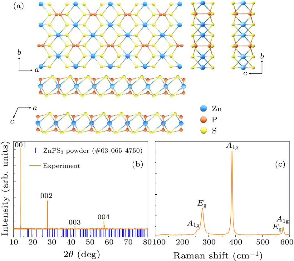
Fig. 1. (a) Schematic crystal structure of ZnPS$_{3}$. Blue, orange and yellow spheres represent Zn, P and S atoms, respectively. (b) Single-crystal XRD pattern of ZnPS$_{3}$. (c) Raman spectrum of ZnPS$_{3}$.
As illustrated in Fig. 1(a), the crystal structure of ZnPS$_{3}$ is monoclinic with a space group of $C12/m1$, which is crystallized in layers composed of a slightly distorted hexagonal network of edge-sharing Zn$^{2+}$ octahedra. The Zn$^{2+}$ ions are coordinated by [P$_{2}$S$_{6}$]$^{4-}$ polyanions. The layers are stacked along the $c$-axis and separated by a vdW gap of 6.73 Å. Figure 1(b) shows the XRD pattern that includes only one array of single-orientation diffractions, highly consistent with the (00$l$) diffractions of powdered ZnPS$_{3}$ (PDF No. 03-065-4750),[15] indicating significant preferential orientation and a layered crystal structure along the $c$ axis. Raman spectroscopy was further performed for structural characterization. As shown in Fig. 1(c), the Raman spectrum collected in the range of 100–600 cm$^{-1}$ reveals several characteristic vibration modes from [P$_{2}$S$_{6}$]$^{4-}$ clusters and zinc cations. The peaks located at 257, 386 and 576 cm$^{-1}$ are identified as the $A_{1g}$ modes and those at 276 and 567 cm$^{-1}$ are the $E_{g}$ modes, respectively. The vibrations around 600 cm$^{-1}$ are attributed to metal cations and the rest are from the [P$_{2}$S$_{6}$]$^{4-}$ clusters, which is in good agreement with previous research.[16] Combining the XRD and Raman characterizations, the as-grown flakes are pure ZnPS$_{3}$. Copper or cobalt intercalation was further introduced into the pristine ZnPS$_{3}$ using the solvent-based method. Figures 2(a) and 2(b) show the comparative optical images of pristine and Co-intercalated ZnPS$_{3}$, respectively, and Figs. 2(c) and 2(d) for pristine and Cu-intercalated ZnPS$_{3}$, respectively. Distinct color changes can be observed after intercalation, suggesting that the intercalation is effective and successful. To analyze the chemical components, the EDS experiment was carried out on the intercalated sample. The panels in Fig. 2(e), respectively, show the mapping data of Zn, P, S, Cu and the total for a selected area of the substrate, complemented by an atomic ratio table taken on an intercalated flake. An obvious signal from Cu atoms is detected, in addition to the signal from Zn, P and S, which confirms the presence of Cu in the sample. The uniform distribution of Cu indicates that besides the areas covered by ZnPS$_{3}$ flakes it still remains on the bare substrate. This is reasonable for a solvent-soaking method. Whether the dopant is indeed inserted in the sample or only adheres to the sample surface can be confusing. The following electrical measurements will reveal clear changes in transport and clarify this confusion. The morphological and EDS characterizations were also taken for the Co-intercalated sample. Obvious color changes were observed [Fig. 2(b)] but no cobalt atoms were detected, which may be due to the slight amount of Co doping. Nevertheless, the transport measurement results presented in the following still confirm a drastic change in conductivity and the effectiveness of Co intercalation.
cpl-38-5-057304-fig2.png
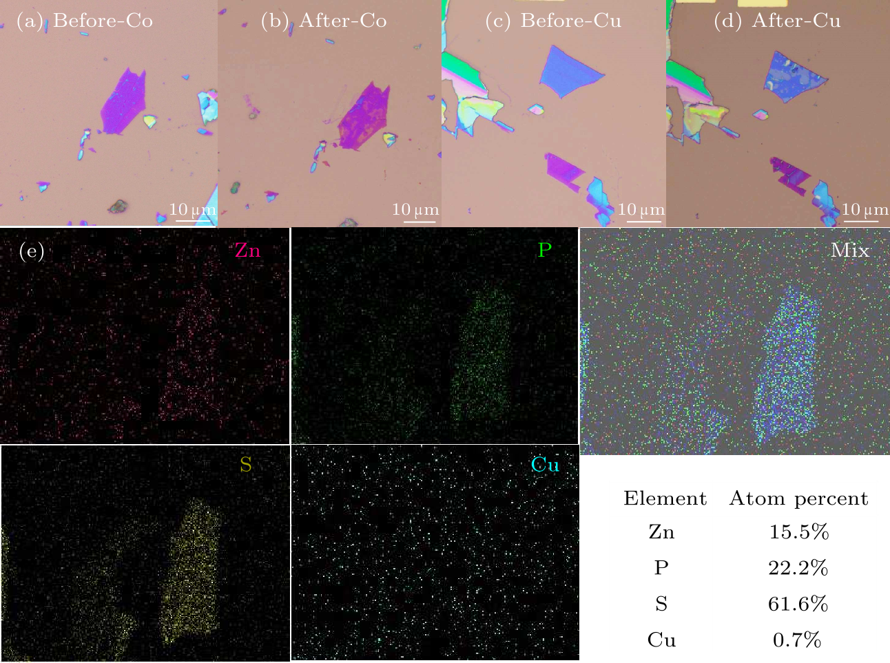
Fig. 2. Optical images of ZnPS$_{3}$ (a) before and (b) after intercalation with Co. Optical images of ZnPS$_{3}$ (c) before and (d) after intercalation with Cu. (e) EDS mapping data of Zn, P, S, Cu and the total for a selected area of the substrate, respectively, and an atomic ratio table taken on the Cu-intercalated flake.
cpl-38-5-057304-fig3.png
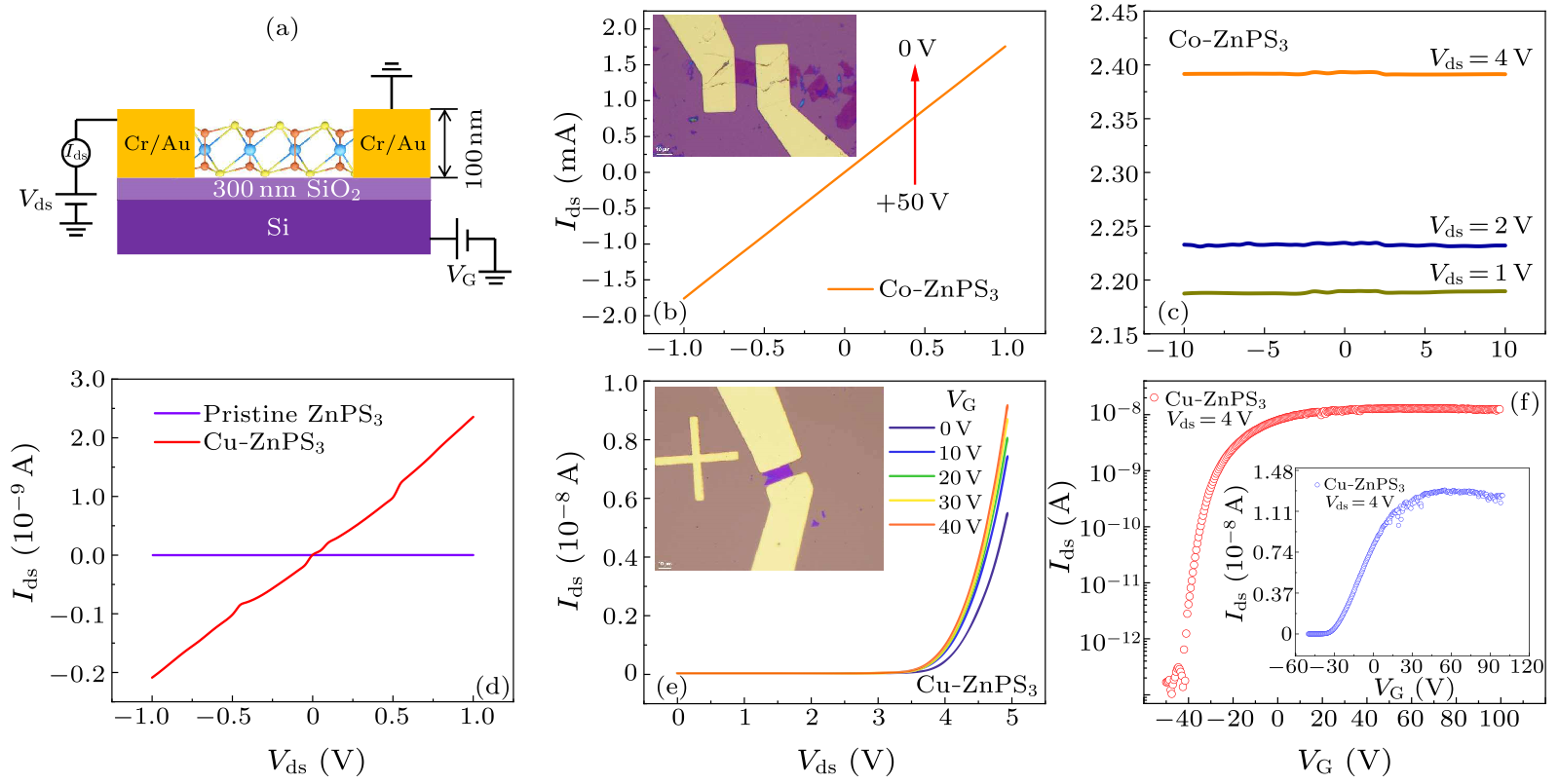
Fig. 3. (a) Cross-section view of the intercalated ZnPS$_{3}$ FET devices. (b) $I_{\rm ds}$–$V_{\rm ds}$ output curves of Co-ZnPS$_{3}$ FET with $V_{\rm G}$ varied from 0 to 50 V. Inset: optical image of Co-ZnPS$_{3}$ device (scale bar is 10 µm). (c) $I_{\rm ds}$–$V_{\rm G}$ transfer curve of Co-ZnPS$_{3}$ FET device with $V_{\rm ds} = 1$ V, 2 V and 4 V, respectively. (d) $I_{\rm ds}$–$V_{\rm ds}$ curves for pristine ZnPS$_{3}$ crystal and Cu-ZnPS$_{3}$, respectively. (e) $I_{\rm ds}$–$V_{\rm ds}$ curves of Cu-ZnPS$_{3}$ FET with $V_{\rm G}$ varied from 0 to 40 V. Inset: optical image of Cu-ZnPS$_{3}$ device (scale bar is 10 µm). (f) $I_{\rm ds}$–$V_{\rm G}$ curve in semilog scale of Cu-ZnPS$_{3}$ FET device with $V_{\rm ds} = 4$ V. Inset: normal scale.
To further check the actual degree of intercalations and investigate the effect of intercalations on the electrical transport, the FET devices of the intercalated flakes were prepared and tested. Figure 3(a) shows a typical schematic diagram of the FET device. The Co-ZnPS$_{3}$ device [see the inset of Fig. 3(b) for the optical image] is first tested by applying a drain-source bias $V_{\rm ds}$ to a pair of metal electrodes and a gate voltage $V_{\rm G}$ to the Si substrate. The $I_{\rm ds}$–$V_{\rm ds}$ output curve exhibits a linear and symmetric relation, suggesting an ohmic contact between the metal electrodes and Co-ZnPS$_{3}$ sample [Fig. 3(b)]. Note that the device current $I_{\rm ds}$ is independent of the gate voltage $V_{\rm G}$ (varied from 0 to 50 V), demonstrating a metallic behavior. Due to the metallic properties of Co-ZnPS$_{3}$ channel, no gating effect is observed when the gate voltage sweeps from $-10$ to 10 V [Fig. 3(c)]. We have further estimated the electrical conductivity of Co-ZnPS$_{3}$, namely about $8\times 10^{4}$ S/m, a value comparable to other 2D metallic materials (Table 1) such as hydrogen arc discharge exfoliated graphene whose conductivity is about $2\times 10^{5}$ S/m.[14] Such a drastic change in transport from an insulator to a highly conductive metal confirms the effective intercalation of Co, although no observation of Co atoms in the above characterizations. The high conductivity of Co-ZnPS$_{3}$ could be useful for many interesting applications such as vdW metal electrodes and building bricks of metal-semiconductor homojunction.
Table 1. Comparison of the electrical conductivity of Co-ZnPS$_3$ and other 2D materials.
Materials Method Electrical conductivity References
Pristine ZnPS$_{3}$ CVT Insulator [8]
Co-ZnPS$_{3}$ Solvent method $\sim$$8\times 10^{4}$ S/m This work
Graphene Hydrogen arc discharge $\sim$$2\times 10^{5}$ S/m [14]
1T-MoS$_{2}$ Chemical exfoliation $\sim$$10^{3}$–10$^{4}$ S/m [17]
Antimonene vdW epitaxial growth $\sim$$1.6\times 10^{4}$ S/m [18]
1T-VS$_{2}$ CVD $\sim$$3\times 10^{5}$ S/m [19]
Co-SnS$_{2}$ Solvent method $\sim$$1.67\times 10^{6}$ S/m [3]
Table 2. Comparison of the carrier mobility of Cu-ZnPS$_3$ and other 2D materials.
Materials Method Type Carrier mobility (cm$^{2}\cdot$V$^{-1}\cdot$s$^{-1}$) References
Pristine ZnPS$_{3}$ CVT Insulator [8]
Cu-ZnPS$_{3}$ Solvent method n-type 0.03 This work
MoS$_{2}$ Mechanical exfoliation n-type 0.1–10 [20]
MoS$_{2}$ CVD on Corning Gorilla Glass n-type 0.14 [21]
WSe$_{2}$ CVD p-type 0.2 [22]
2H-MoTe$_{2}$ Mechanical exfoliation Ambipolar $0.02$ [23,24]
NiPS$_{3}$ Mechanical exfoliation n-type 0.5–1 [25]
MnPS$_{3}$ Mechanical exfoliation p-type $\mathrm{2.7\times }{10}^{-3}$ [26]
Cu-SnS$_{2}$ Solvent method ionic liquid gated p-type $40$ [3]
We then study the Cu-ZnPS$_{3}$ FET device following the same method. Figure 3(d) shows the $I_{\rm ds}$–$V_{\rm ds}$ curves within $\pm 1$ V for pristine ZnPS$_{3}$ and Cu-ZnPS$_{3}$, respectively. Compared with the pristine ZnPS$_{3}$, the conductivity of Cu-ZnPS$_{3}$ is greatly enhanced. As shown in Fig. 3(f), the current $I_{\rm ds}$ increases with the increasing gate voltage $V_{\rm G}$, a typical characteristic of transfer curve of an n-type channel, suggesting that the Cu-intercalated sample has become an n-type semiconductor. The OFF-current is as low as 10$^{-13}$ A, which is a useful feature for making low-power logic circuits. The ON-current is 10$^{-8}$ A when the source-drain bias voltage is 4 V. The estimated ON/OFF current ratio is about 10$^{5}$, which can be compared to MoS$_{2}$ grown on multicomponent glass[21] (Table 2). Note that the nonlinear $I_{\rm ds}$–$V_{\rm ds}$ output curves suggest a Schottky barrier formed between the Cr/Au metal contacts and the sample [Fig. 3(e)]. For a two-terminal device, the presence of Schottky barrier usually reduces the device performance. Thus, the intrinsic transport performance of Cu-ZnPS$_{3}$ should be better. An improved metal contact with a suitable work function deserves further research.
The field-effect mobility can be extracted from the transfer curve using the equation $$ \mu =\frac{dI_{\mathrm{ds}}}{dV_{\rm G}}\times \frac{L}{W\cdot V_{\mathrm{ds}}\cdot C_{i}},~~ \tag {1} $$ where $\mu$ is the mobility, $W$ is the channel width, $L$ is the channel length and $C_{i}$ is the capacitance between the channel and the back gate per unit area $[C_{i}=(\varepsilon_{0}\varepsilon_{\rm r})/d = 1.1\times 10^{-4}$ F/m$^{2}$ for $\varepsilon_{\rm r} = 3.9$, $\varepsilon_{0} = 8.85\times 10^{-12}$ F/m and $d = 300$ nm]. The calculated mobility is $3\times 10^{-2}$ cm$^{2}\cdot$V$^{-1}\cdot$s$^{-1}$, which is a typical value for a semiconductor. This relatively low mobility may be linked to the poor contact with the metal electrodes, as reported for some 2D semiconductors.[20] The mobility can be improved in top-gated devices by depositing high-$\kappa$ dielectric materials such as HfO$_{2}$ in future work.[27] Although these revealed parameters are not good enough for high-performance FET applications, the realization of a typical semiconductor and a metallic state in the same 2D material enables a possibility to fabricate metal-semiconductor homojunction. Taking into account the insulating state of pristine ZnPS$_{3}$, the application range can even be further expanded. The insulating ZnPS$_{3}$ can be utilized as an insulating layer or a gate material. The metallic Co-ZnPS$_{3}$ can serve as metallic contacts or an electron storage layer. Combined with Cu-ZnPS$_{3}$, a feasible n-type semiconductor, a variety of functional devices can be designed and put into practice on one piece of ZnPS$_{3}$ flake, such as memristors.[28] In summary, we have demonstrated that the insulating pristine ZnPS$_{3}$ can be transformed into a highly conductive metal and an n-type semiconductor by intercalating Co and Cu atoms, respectively. The FET devices have been prepared via an ultraviolet exposure lithography technique, with the intercalated ZnPS$_{3}$ flakes as conductive channel and SiO$_{2}$ as back gate insulator. The Co-ZnPS$_{3}$ device exhibits an electrical conductivity of $8\times 10^{4}$ S/m, which is comparable to the conductivity of hydrogen arc discharge exfoliated graphene. The Cu-ZnPS$_{3}$ FET reveals a current ON/OFF ratio of 10$^{5}$ and a mobility of $3\times 10^{-2}$ cm$^{2}\cdot$V$^{-1}\cdot$s$^{-1}$. The realization of an insulator, a typical semiconductor and a metallic state in the same 2D material provides an opportunity to fabricate atomically seamless n-metal homojunction and other in-plane electronic functional devices.
References Integration of bulk materials with two-dimensional materials for physical coupling and applicationsTwo-Dimensional Dielectric Nanosheets: Novel Nanoelectronics From Nanocrystal Building BlocksSpatially controlled doping of two-dimensional SnS2 through intercalation for electronicsMetal Thio- and Selenophosphates as Multifunctional van der Waals Layered MaterialsNature of the oxidizing centres in transition metal phosphorus trisulfides MPS3 (M = Fe, Ni)Stilbazolium-MPS3 Nanocomposites with Large Second-Order Optical Nonlinearity and Permanent MagnetizationThe intercalation of 1,10-phenanthroline into layered NiPS 3 via iron dopant seedingElectrical conductivity of layered transition-metal phosphorus trisulfide crystalsMagnetic properties and specific heat of MPS3 (M=Mn, Fe, Zn)Vibrational study of layered ZnPS3 compounds intercalated with [Co(η5 -C5H5)2+] and [Cr(η6 -C6H6)2+] CATIONSSecond-order Jahn—Teller effect in CdPS3 and ZnPS3 demonstrated by a non-harmonic behaviour of Cd2+ and Zn2+ d10 ionsChemical Intercalation of Zerovalent Metals into 2D Layered Bi 2 Se 3 NanoribbonsOptical transmission enhacement through chemically tuned two-dimensional bismuth chalcogenide nanoplatesSynthesis of Graphene Sheets with High Electrical Conductivity and Good Thermal Stability by Hydrogen Arc Discharge ExfoliationStructure determination of ZnPS3Layered Metal Thiophosphite Materials: Magnetic, Electrochemical, and Electronic PropertiesMetallic 1T phase MoS2 nanosheets as supercapacitor electrode materialsTwo-dimensional antimonene single crystals grown by van der Waals epitaxyMetallic Vanadium Disulfide Nanosheets as a Platform Material for Multifunctional Electrode ApplicationsSingle-layer MoS2 transistorsLow-Power and Ultra-Thin MoS 2 Photodetectors on GlassLarge-area synthesis of monolayer WSe 2 on a SiO 2 /Si substrate and its device applicationsOrigin of Noise in Layered MoTe 2 Transistors and its Possible Use for Environmental SensorsAmbipolar MoTe 2 Transistors and Their Applications in Logic CircuitsField Effect Transistor Based on Layered NiPS 3Bulk and few-layer MnPS 3 : a new candidate for field effect transistors and UV photodetectorsEnhancement of Carrier Mobility in Semiconductor Nanostructures by Dielectric EngineeringNonvolatile Memories Based on Graphene and Related 2D Materials
[1] Bae S H et al. 2019 Nat. Mater. 18 550
[2] Osada M and Sasaki T 2012 Adv. Mater. 24 210
[3] Gong Y et al. 2018 Nat. Nanotechnol. 13 294
[4] Susner M A et al. 2017 Adv. Mater. 29 1602852
[5] Brec R et al. 1987 J. Power Sources 20 205
[6] Lacroix P G et al. 1994 Science 263 658
[7] Ma X et al. 2020 Chem. Commun. 56 4603
[8] Ichimura K and Sano M 1991 Synth. Met. 45 203
[9] Takano Y et al. 2004 J. Magn. Magn. Mater. 272 E593
[10] Sourisseau C, Forgerit J P, and Mathey Y 1983 J. Phys. Chem. Solids 44 119
[11] Boucher F, Evain M, and Brec R 1994 J. Alloys Compd. 215 63
[12] Koski K J et al. 2012 J. Am. Chem. Soc. 134 13773
[13] Yao J et al. 2014 Nat. Commun. 5 5670
[14] Wu Z S et al. 2009 ACS Nano 3 411
[15] Prouzet E, Ouvrard G, and Brec R 1986 Mater. Res. Bull. 21 195
[16] Mayorga-Martinez C C et al. 2017 ACS Appl. Mater. & Interfaces 9 12563
[17] Acerce M, Voiry D, and Chhowalla M 2015 Nat. Nanotechnol. 10 313
[18] Ji J et al. 2016 Nat. Commun. 7 13352
[19] Ji Q et al. 2017 Nano Lett. 17 4908
[20] Radisavljevic B et al. 2011 Nat. Nanotechnol. 6 147
[21] Nasr J R et al. 2020 ACS Nano 14 15440
[22] Huang J et al. 2015 Nanoscale 7 4193
[23] Lin Y F et al. 2015 Adv. Mater. 27 6612
[24] Lin Y F et al. 2014 Adv. Mater. 26 3263
[25] Jenjeti R T et al. 2018 Sci. Rep. 8 8586
[26] Kumar R et al. 2019 J. Mater. Chem. C 7 324
[27] Jena D and Konar A 2007 Phys. Rev. Lett. 98 136805
[28] Bertolazzi S et al. 2019 Adv. Mater. 31 1806663