Chinese Physics Letters, 2021, Vol. 38, No. 10, Article code 107403 Photoemission Spectroscopic Evidence of Multiple Dirac Cones in Superconducting BaSn$_3$ Zhe Huang (黄喆)1,2,3, Xianbiao Shi (石贤彪)4,5, Gaoning Zhang (张高宁)3, Zhengtai Liu (刘正太)1, Soohyun Cho1, Zhicheng Jiang (江志诚)1, Zhonghao Liu (刘中灏)1, Jishan Liu (刘吉山)1*, Yichen Yang (杨逸尘)1, Wei Xia (夏威)3,6, Weiwei Zhao (赵维巍)4,5, Yanfeng Guo (郭艳峰)3*, and Dawei Shen (沈大伟)1,2* Affiliations 1Center for Excellence in Superconducting Electronics, State Key Laboratory of Functional Materials for Informatics, Shanghai Institute of Microsystem and Information Technology, Chinese Academy of Sciences, Shanghai 200050, China 2Center of Materials Science and Optoelectronics Engineering, University of Chinese Academy of Sciences, Beijing 100049, China 3School of Physical Science and Technology, ShanghaiTech University, Shanghai 201210, China 4State Key Laboratory of Advanced Welding and Joining, Harbin Institute of Technology, Shenzhen 518055, China 5Flexible Printed Electronics Technology Center, Harbin Institute of Technology, Shenzhen 518055, China 6ShanghaiTech Laboratory for Topological Physics, ShanghaiTech University, Shanghai 201210, China Received 14 July 2021; accepted 13 September 2021; published online 26 September 2021 Supported by the National Key R$\&$D Program of China (Grant No. 2016YFA0300204), the National Natural Science Foundation of China (Grant Nos. U2032208 and 11874264), and the Natural Science Foundation of Shanghai (Grant No. 14ZR1447600). Y. F. Guo acknowledges the starting grant of ShanghaiTech University and the Program for Professor of Special Appointment (Shanghai Eastern Scholar). Part of this research used Beamline 03U of the Shanghai Synchrotron Radiation Facility, which is supported by ME2 project (Grant No. 11227902) from the National Natural Science Foundation of China. ZJW was supported by the National Natural Science Foundation of China (Grant No. 11974395), the Strategic Priority Research Program of Chinese Academy of Sciences (Grant No. XDB33000000), and the Center for Materials Genome. The authors also thank the support from Analytical Instrumentation Center, SPST, ShanghaiTech University (Grant No. SPST-AIC10112914).
*Corresponding authors. Email: jishanliu@mail.sim.ac.cn; guoyf@shanghaitech.edu.cn; dwshen@mail.sim.ac.cn
Citation Text: Huang Z, Shi X B, Zhang G N, Liu Z T, and Cho S et al. 2021 Chin. Phys. Lett. 38 107403    Abstract Signatures of topological superconductivity (TSC) in superconducting materials with topological nontrivial states prompt intensive researches recently. Utilizing high-resolution angle-resolved photoemission spectroscopy and first-principles calculations, we demonstrate multiple Dirac fermions and surface states in superconductor BaSn$_3$ with a critical transition temperature of about 4.4 K. We predict and then unveil the existence of two pairs of type-I topological Dirac fermions residing on the rotational axis. Type-II Dirac fermions protected by screw axis are confirmed in the same compound. Further calculation for the spin helical texture of the observed surface states originating from the Dirac fermions gives an opportunity for realization of TSC in one single material. Hosting multiple Dirac fermions and topological surface states, the intrinsic superconductor BaSn$_3$ is expected to be a new platform for further investigation of topological quantum materials as well as TSC. DOI:10.1088/0256-307X/38/10/107403 © 2021 Chinese Physics Society Article Text The long-sought topological superconductivity (TSC) has attracted vast attention and has been boomingly developed in the last decade, which were spurred by the potential realization of Majorana fermions.[1–7] In this context, there has been an explosion of proposals to search for novel materials hosting TSC, including intrinsic odd-parity superconductors[8–11] and heterostructures taking advantage of the superconducting proximity effect of spin helical surface states in topological insulators (TIs)[12] or spin polarization in Rashba semiconductors[13–17] to conventional s-wave pairing in superconductors. However, for the former strategy, the paring symmetry of devised candidates for p-wave superconductors still remains elusive.[18–25] As for the case of heterostructures, the utilization of spin-triplet pairing feasible at interfaces was hindered by the intricacy of fabrication and the disturbance of interface physics.[26–44] Some crystals have been proposed to be topological superconductors theoretically and experimentally.[45–49] Recent researches reported evidences of s-wave superconductors hosting TI states with spin polarized surface states and Majorana zero mode in the vortex core, suggestive of a new way to realize TSC in one single material.[50–56] In addition, s-wave superconductors with topological Dirac semimetal states have also been proposed as candidates for TSC,[57,58] taking into account of the helical surface states around the Fermi level ($E_{\rm F}$) brought by Dirac bands. Experimentally, the possible unconventional superconductivity has been reported to be induced by point contact[59,60] or high pressure[61] in the prototype Dirac semimetal Cd$_3$As$_2$. However, such extreme external conditions would prohibit further investigation and application of TSC, and searching for intrinsic superconducting topological Dirac semimetal is highly desired. Recently, superconducting compounds ASn$_3$ (A = Ca or Ba) were predicted to host topological semimetal states.[62–66] Studies on the topology in the weak coupling superconductor CaSn$_3$ propose that it hosts topological nodal-line semimetal states in the absence of spin-orbital coupling (SOC) and would evolve Weyl nodes with SOC.[62–64] However, its relatively complicated band structure impedes the direct investigation of the nontrivial band topology therein. Fascinatingly, first-principles calculations suggest that the electronic band structure of BaSn$_3$ harbors multiple simple topological Dirac semimetal states, and type-II bulk superconductivity has been experimentally confirmed with an onset superconducting temperature $T_{\rm c}^{\rm onset} \sim 4.4$ K.[65,67] Moreover, de Haas-van Alphen (dHvA) measurements on this compounds have provided evidence on the possible nontrivial Berry phase associated with the proposed type-II Dirac point around $E_{\rm F}$, making it a good candidate to realize TSC and Majorana fermions.[65] So far, the direct confirmation of proposed multiply Dirac fermions in the low-lying electronic structure is still lack. In this work, we predict and then directly identify the multiple Dirac fermions in the superconducting BaSn$_3$ by employing first-principles calculations and high-resolution angle-resolved photoemission spectroscopy (ARPES). Our ARPES result on the unique (100) cleavage plane verifies the existence of two pairs of type-I three-dimensional Dirac points (DPs) residing on the rotational axis. In the same compound, we discover type-II DPs protected by the screw axis. Moreover, we deduce that the observed surface states with predicted spin helical texture could induce the possible TSC in one single material. Our experimental result is complementary to the previous transport measurements, and consolidates the evidence on the nontrivial topological bands and two types of Dirac fermions in BaSn$_3$. Our findings uncover the topological electronic states in superconducting BaSn$_3$, which may provide a new platform for further studies on the topological quantum materials as well as TSC. High-quality single crystals of BaSn$_3$ were grown with a self flux method. Details on the sample growth and characterization can be found elsewhere.[65] High-resolution ARPES measurements were performed at 03U beam line of Shanghai Synchrotron Radiation Facility (SSRF)[68] and 13U beam line of National Synchrotron Radiation Laboratory (NSRL), respectively. Both end stations are equipped with Scienta Omicron DA30 electron analyzers. Considering the sensitivity of BaSn$_3$ to water in air, all samples were meticulously selected and prepared in the glove box first, and then cleaved along both the (001) and (100) cleavage planes. All ARPES data were taken at 15 K in an ultrahigh vacuum better than $8.0 \times 10^{-11}$ mbar. The angular and the energy resolutions were set to 0.2$^\circ$ and 6–20 meV (depending on the incident photon energies), respectively. First-principles calculations were performed within the framework of the projector augmented wave (PAW) method and selected the generalized gradient approximation (GGA) with Perdew–Burke–Ernzerhof (PBE) type, as encoded in the Vienna ab initio simulation package (VASP). A kinetic energy cutoff of 500 eV and a $\varGamma$-centered $k$-mesh of $6 \times 6 \times 9$ were utilized for all calculations. During self-consistent convergence and structural relaxation, the energy and force difference criterion were defined as $10^{-6}$ eV and 0.01 eV/Å. SOC was considered in a self-consistent manner. The WANNIER90 package was adopted to construct Wannier functions from the first-principles results. Topological properties calculations were carried out using the WANNIERTOOLS code.
cpl-38-10-107403-fig1.png
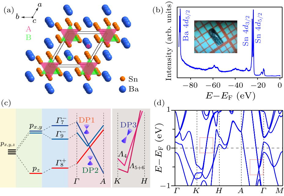
Fig. 1. (a) Crystal structure of BaSn$_3$. (b) Core-level photoemission spectrum clearly shows the characteristic Ba 4$d$ and Sn 4$d$ peaks. Inset: photograph of the high-quality BaSn$_3$ single crystal with shiny surface used for ARPES measurement. (c) Schematic illustration of $p$-orbital energy level evolution to form the type-I DPs. Right column: The band structure of type-II DPs. The symmetry of energy levels is labeled by the IRs. (d) The calculated band structure of BaSn$_3$.
BaSn$_3$ crystallizes in the hexagonal Ni$_3$Sn structure with the space group $P6_{3}mmc$ (No. 194).[67] Two hexagonal layers containing Ba and Sn atoms are stacked in an $A$–$B$–$A$–$B$ sequence to form a close-packed structure as schematically illustrated in Fig. 1(a). Thus, the (100) cleavage plane is easier to be obtained than the (001) one [Fig. 1(a)], which provides a good opportunity to directly observe both types of DPs. Previous single-crystal x-ray diffraction (XRD) and energy dispersive spectroscopy (EDS) measurements have confirmed the high crystalline quality and accurate stoichiometric proportion of our samples.[65] Furthermore, our core-level photoemission measurements further confirm the chemical composition of BaSn$_3$ [Fig. 1(b)], showing sharp Ba 4$d$ and Sn 4$d$ orbital peaks. We note that our samples show a superconducting transition temperature of 4.4 K and behave as a type-II superconductor in our previous report.[65] After cleaved, the sample shows typical flat and shining surface as illustrated in the inset of Fig. 1(b). The crystal structure of BaSn$_3$ respects both the inversion and $C_3$ rotation symmetries, protecting the predicted topological DPs.[65,67] Here, the nontrivial topological band structure of BaSn$_3$ originates from the band inversion within the $p$ orbitals of Sn as shown in Fig. 1(c). When the crystal-field splitting is under consideration, the $p$ orbitals splits into $p_{x,y}$ and $p_z$ possessing different energies. When the SOC participates in it, the in-plane bands from $p_{x,y}$ orbital further splits into bands which belongs to $\varGamma_7^-$ and $\varGamma_9^-$ irreducible representations (IR) and cross with each other. Meanwhile, the $\varGamma_7^-$ band crosses with the $\varGamma_8^+$ band originating from the $p_z$ orbital. Due to different IRs of these crossing bands, two type-I DPs marked as DP1 and DP2 form along $\varGamma$–$A$ direction. Protected by the inversion and time reversal symmetry, all bands in BaSn$_3$ is doubly degenerate. Therefore, the DP1 and DP2 are fourfold degenerate and protected by the additional $C_3$ rotation symmetry to prevent the gap from opening due to the SOC effect. More interestingly, along the $K$–$H$ direction, there is an unavoidable crossing between two bands forming the strongly tilted type-II Dirac fermion labeled as DP3 as illustrated in the right column of Fig. 1(c). The symmetry analysis indicates that two crossing bands belong to $\varLambda_4$ and $\varLambda_{5+6}$, respectively. Figure 1(d) shows total band dispersions along high-symmetry directions with SOC. The electronic structure near $E_{\rm F}$ is mainly dominated by Sn 5$p$ orbitals [Details in Note 1 in the Supplemental Material (SM)]. We highlight the bands related to topological DPs by red boxes. Experimentally, we first investigated the overall electronic structure of BaSn$_3$. The three-dimensional Brillouin zone (BZ) of BaSn$_3$ is illustrated in Fig. 2(a), in which plotted black dots indicate high-symmetry points. The directions of $k_x$, $k_y$ and $k_z$ are defined to parallel to $\varGamma$–$M$, $\varGamma$–$K$ and $\varGamma$–$A$, respectively. To trace the evolution of the bulk electronic structures and determine the high symmetry surface, systematic photon energy dependent measurements were performed (photon energy ranged from 41 eV to 91 eV). Here, we discuss the $k_x$-momentum determination. Since the surface of the measured sample breaks the translational symmetry along out-of-plane direction, the perpendicular momentum components of the photoelectron ($k_\perp^f$) and the initial electron ($k_\perp^i$) are not equivalent. Although we can not get the out-of-plane momentum directly as the in-plane momentum ($k_z$ and $k_y$), it is helpful to determine the $k_x$ momentum based on the nearly free-electron approximation for final states,[65] $$ k_{\operatorname{\perp}}^{\operatorname{i}} = \sqrt{2m(E_{\operatorname{kin}}\cos^{\operatorname{2}}\theta) +V_{\operatorname{0}}}/\hbar,~~ \tag {1} $$ where $V_0$ is the inner potential which is a constant and can be defined by fitting the periodicity of different photon energy measurements. As shown in Figs. 2(c) and 2(d), the clear periodic patterns were observed in both $k_x$–$k_z$ planes at $E_{\rm F} - 0.3$ eV and $E_{\rm F} - 0.5$ eV. We got the inner potential $V_0 = 13$ eV in BaSn$_3$ from the $k_x$ dependent photoemission intensity plots. Thus, we can determine the exact value of $k_\perp$ and the corresponding high symmetry points and surfaces.
cpl-38-10-107403-fig2.png
Fig. 2. (a) Bulk BZ with high-symmetry points. Two planes labeled as FS1 and FS2 indicate the $k_x = 0$ and $k_x = \pi$, respectively. (b) Stack of CECs in the $k_y$–$k_z$ plane showing the lower part of Dirac cone. [(c), (d)] Photoemission intensity plots in the $k_x$–$k_z$ plane at $E_{\rm F} -0.3$ eV and $E_{\rm F} -0.5$ eV, respectively. [(e), (f)] Calculated bulk FSs in the high-symmetry plane FS1 at $E_{\rm F}$ and $E_{\rm F}-0.5$ eV, respectively. [(g), (h)] Photoemission intensity plots at $E_{\rm F}$ and $E_{\rm F}-0.5$ eV, showing CECs on FS1 indicated in (a). (i) Calculated bulk FSs in the high-symmetry plane FS2 at $E_{\rm F}$. (j) Photoemission intensity plots at $E_{\rm F}$ in FS2. The data were recorded on the (100) cleavage plane with linearly horizontal polarized photons. (g)–(h) Taken at 87 eV. (j) Taken at 71 eV.
The photoemission intensity maps of constant energy contours (CECs) at $E_{\rm F}$ on in-plane FS1 and FS2 [Figs. 2(g) and 2(j)] indicate the Fermi surfaces (FSs) on the $k_x = 0$ and $k_x = \pi$, respectively, as schematically illustrated in Fig. 2(a), which are in agreement with calculations [Figs. 2(e) and 2(i)]. From the detailed investigation of CECs on FS1 at different binding energies, we could recognize both type-I Dirac points DP1 and DP2. One hole-like band $\alpha$ belonging to $\varGamma_7^-$ and two electron-like bands $\beta$, $\gamma$ belonging to $\varGamma_9^-$, $\varGamma_8^+$ could be identified in both the calculation [Fig. 2(e)] and experimental result [Fig. 2(g)] near $\varGamma$ at $E_{\rm F}$. With the increase of binding energy, the hole pocket from $\alpha$ band near $\varGamma$ extends, while the electron one from $\beta$ band shrinks. More details on CECs at different binding energies can be found in Note 2 of the SM.[64] As shown in Fig. 2(h), the above two pockets finally overlap at $E_{\rm F} - 0.5$ eV where the DP1 is form, in agreement with the theory [Fig. 2(f)]. Meanwhile, from the stack of calculated CECs results at 0.6, 0.7 and 0.8 eV below $E_{\rm F}$ [Fig. 2(b)], we could identify the evolution of the lower part of the Dirac cone from DP2 located at $\sim $0.6 eV below $E_{\rm F}$. Next, we focus on the FS1 plane to identify the two types of Dirac fermions along $\varGamma$–$A$ and $K$–$H$ high symmetry directions [cut 1 and cut 3 in Fig. 3(a)]. The band calculation along $\varGamma$–$A$ direction indicates that DP1 is located at $\sim 0.5$ eV below $E_{\rm F}$ where $\alpha$ and $\beta$ bands cross, while the DP2 is located at $\sim 0.6$ eV below $E_{\rm F}$ where $\alpha$ and $\gamma$ bands cross [Fig. 3(b)]. To search for the theoretically proposed DP1 and DP2, we measured the band dispersions along the $\varGamma$–$A$, namely, cut 1 as shown in Fig. 3(c). The ARPES intensity plot exhibits three bands and two crossing points, consistent with the theoretical prediction. Since BaSn$_3$ respects both the inversion and time-reversal symmetries, these two intersections between $\alpha/\beta$ and between $\alpha/\gamma$ are both fourfold degenerate. The additional $C_3$ symmetry protects Dirac fermions from gapping out, finally forming two bulk topological nontrivial type-I DPs marked as DP1 and DP2. To further locate these two DPs, we display momentum distribution curves (MDCs) [Fig. 3(c)(ii)] of the region in the red box and the enlarged second derivative intensity plot [Fig. 3(c)(ii)] of the region in the white box. Here, the calculated band structure has been appended on top of the experimental data, from which we can identify the DP1 situated at $E_{\rm F} - 0.5$ eV, and DP2 at $E_{\rm F} - 0.6$ eV. Thus, we directly demonstrate and locate both predicted type-I DPs in BaSn$_3$.
cpl-38-10-107403-fig3.png
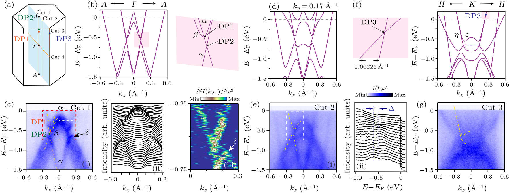
Fig. 3. (a) Bulk BZ with orange lines indicating the location of cuts 1–4. (b) Calculated band structure along $\varGamma$–$A$ high-symmetry direction with SOC. Right column: the enlarged image of the red box, displaying two pair of type-I DPs. (c) (i) Photoemission intensity plots of band dispersions along cut 1, (ii) the enlarged MDCs plot of region in the red box, (iii) the second derivative intensity of region in the white box. (d) Calculated band structure along cut 2 with SOC. (e) (i) Photoemission intensity plots of band dispersions along cut 2, (ii) EDCs of region in the white box. (f) Calculated band structure along $K$–$H$ high-symmetry direction with SOC. Left column: the enlarged broadening image of the red box, displaying tilted type-II DP. (g) Photoemission intensity plots of band dispersions along cut 3. The ARPES data were recorded on the (100) cleavage surface with 53 eV in (c) and 28 eV in [(e), (g)] under linearly horizontal polarization.
To further trace the band structure related to DP1 and DP2, we measured detailed band dispersions on the FS1 plane parallel to $\varGamma$–$A$ as illustrated in Fig. 3(a). The experimental band dispersions at $k_y = 0$ Å$^{-1}$ exhibit one hole-like band $\alpha$, one W-shaped band $\beta$ and one V-shaped band $\gamma$ [Fig. 3(c)], with two crossing points DP1 and DP2, respectively. Note that the M-shaped band $\delta$ which is caused by the electronic intensity from other high-symmetry direction parallel to $\varGamma$–$A$ direction does not participate in the formation of DPs according to our slab calculation [see details in Note 3 of SM]. Since all DPs along $\varGamma$–$A$ are protected by the $C_3$ rotation symmetry, upon sliding the cut to $k_y = 0.17$ Å$^{-1}$ [cut 2 shown in Fig. 3(a)], which deviates from high symmetry lines, the gaps near two DPs are turned on [Fig. 3(e)], which is consistent with the calculated result [Fig. 3(d)]. Furthermore, the corresponding energy distribution curves (EDCs) for the enlarged region can further reveal the band gap, as shown in Fig. 3(e)(ii). In addition to the two type-I DPs along $\varGamma$–$A$, we found the evidence for the existence of type-II DP along $K$–$H$. Upon further sliding the cut to $k_y = 0.5$ Å$^{-1}$ [cut 3 in Fig. 3(a)], which precisely slices the $K$–$H$ direction, the band structures exhibit one W-shaped band $\epsilon$ and one U-shaped band $\eta$ [Fig. 3(g)], in line with the calculation [Fig. 3(f)]. Since the $\epsilon$ and $\eta$ bands belong to two different IRs $\varLambda_4$ and $\varLambda_{5+6}$, respectively, the unavoidable crossing between them will occur above the $E_{\rm F}$ as calculated in Fig. 3(f). We note that from the enlarged image here, the $\epsilon$ and $\eta$ bands are only 0.00225 Å$^{-1}$ apart from $E_{\rm F}$, beyond the momentum resolution of our photoemission experiments. Thus, we cannot separate the $\epsilon$ and $\eta$ bands at $E_{\rm F}$. The type-II DPs strongly tilting along the $K$–$H$ are protected by the screw axes, inversion and time-reversal symmetry.
cpl-38-10-107403-fig4.png
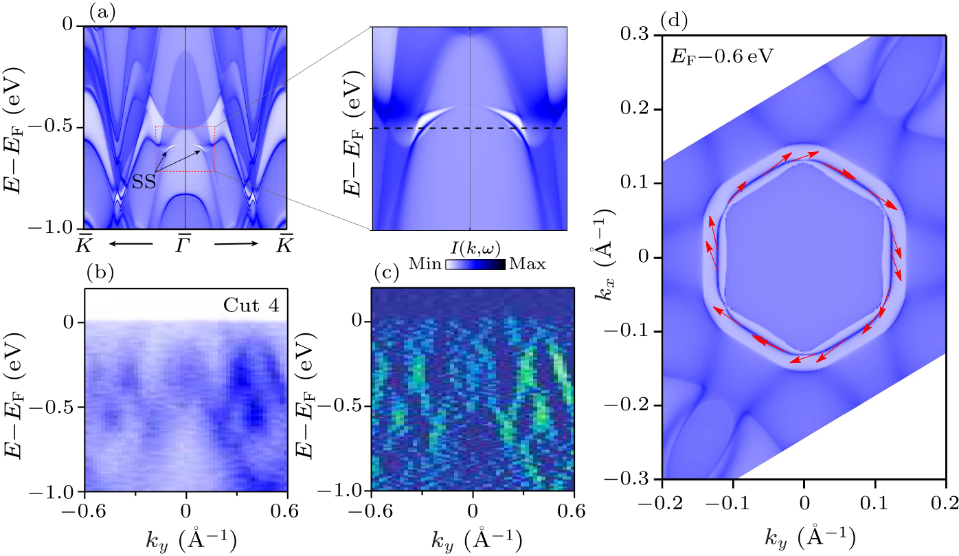
Fig. 4. (a) Calculated topological surface states along $\bar{\varGamma}$–$\bar{K}$ high-symmetry direction. Right column: the enlarged calculated result in the red box. (b) Photoemission intensity plots of band dispersions along $\varGamma$–$K$ high-symmetry direction. The surface states labeled as SS are marked by black arrow. (c) The second derivative plot of (b). The ARPES data were taken with 87 eV under linearly horizontal polarization. (d) Calculated spin texture at 0.6 eV below $E_{\rm F}$, displaying the spin-momentum locking texture.
In Fig. 4, we investigate the topological surface states originating from the observed DP2 and the spin polarized texture. The calculated surface states from the DP2 shown in Fig. 4(a) are marked as SS by black arrows along the $\bar{\varGamma}$–$\bar{K}$ direction. The photoemission intensity plot along $\varGamma$–$K$ high symmetry direction [cut 4 in Fig. 3(a)] shows the evidence of surface states at $\sim $0.6 eV below $E_{\rm F}$, which is consistent with the calculated result. From the second derivative plot of Fig. 4(b), we could recognize the surface states more clearly in Fig. 4(c). To further study the spin texture of these surface states, we calculate the constant-energy plot of spin texture at $E_{\rm F} - 0.6$ eV. These red arrows in Fig. 4(d) show the spin direction of electrons, indicating the characteristic spin-momentum locking texture of these surface states. The coexistence of bulk DPs and spin-helical surface states in superconductor BaSn$_3$ resembles that of iron-based superconductor [e.g., Fe(Te,Se), Li(Fe,Co)As].[57,58] Taking advantage of the proximity effect in momentum space, the possible helical surface states could be induced to get the superconducting order parameter, in which the superconducting gap could be opened and realize the TSC in one single material. Furthermore, the hole doping will lower the $E_{\rm F}$ and make the DPs and surface states closer to the $E_{\rm F}$. Then the FS with mixing parities could form. Therefore, the superconductor BaSn$_3$ with $T_{\rm c} \sim 4.4$ K could be an exciting platform to enrich the potential TSC family. In summary, we have identified the multiple Dirac fermions and related surface states with predicted spin-momentum locking texture in the superconductor BaSn$_3$ by ARPES measurements in association with first-principles calculations. The high resolution ARPES results recognize the dual type-I DPs and provide evidence for the type-II DP complementary to the previous transport measurement. The topological Dirac fermions and surface states make BaSn$_3$ a good platform for exploring the topological quantum materials. Our findings are also beneficial for research on TSCs.
References Topological insulators and superconductorsNew directions in the pursuit of Majorana fermions in solid state systemsIntroduction to topological superconductivity and Majorana fermionsSearch for Majorana Fermions in SuperconductorsMajorana fermions in semiconductor nanowires: fundamentals, modeling, and experimentMajorana quasiparticles in condensed matterTopological superconductors: a reviewThe superconductivity of Sr 2 RuO 4 and the physics of spin-triplet pairingOdd-Parity Topological Superconductors: Theory and Application to Cu x Bi 2 Se 3 Topological odd-parity superconductorsMajorana Fermions and Exotic Surface Andreev Bound States in Topological Superconductors: Application to Cu x Bi 2 Se 3 Superconducting Proximity Effect and Majorana Fermions at the Surface of a Topological InsulatorMajorana fermions in a tunable semiconductor deviceGeneric New Platform for Topological Quantum Computation Using Semiconductor HeterostructuresMajorana Fermions and a Topological Phase Transition in Semiconductor-Superconductor HeterostructuresMajorana zero modes in superconductor–semiconductor heterostructuresTopological superconductivity in hybrid devicesEdge States of Sr 2 RuO 4 Detected by In-Plane Tunneling SpectroscopyObservation of Half-Height Magnetization Steps in Sr2RuO4Superconductivity in Cu x Bi 2 Se 3 and its Implications for Pairing in the Undoped Topological InsulatorObservation of topological order in a superconducting doped topological insulatorTopological Superconductivity in Cu x Bi 2 Se 3 Spin-rotation symmetry breaking in the superconducting state of CuxBi2Se3Thermodynamic evidence for nematic superconductivity in CuxBi2Se3Superconductivity with Topological Surface State in Sr x Bi 2 Se 3Unconventional Josephson Effect in Hybrid Superconductor-Topological Insulator DevicesThe Coexistence of Superconductivity and Topological Order in the Bi 2 Se 3 Thin FilmsFully gapped topological surface states in Bi2Se3 films induced by a d-wave high-temperature superconductorSymmetry protected Josephson supercurrents in three-dimensional topological insulatorsJosephson Supercurrent through the Topological Surface States of Strained Bulk HgTePhase Coherence and Andreev Reflection in Topological Insulator DevicesInduced superconductivity in the quantum spin Hall edgeSignatures of Majorana Fermions in Hybrid Superconductor-Semiconductor Nanowire DevicesThe fractional a.c. Josephson effect in a semiconductor–superconductor nanowire as a signature of Majorana particlesZero-bias peaks and splitting in an Al–InAs nanowire topological superconductor as a signature of Majorana fermionsAnomalous Zero-Bias Conductance Peak in a Nb–InSb Nanowire–Nb Hybrid DeviceSuperconductor-nanowire devices from tunneling to the multichannel regime: Zero-bias oscillations and magnetoconductance crossoverAnomalous Modulation of a Zero-Bias Peak in a Hybrid Nanowire-Superconductor DeviceSpin-resolved Andreev levels and parity crossings in hybrid superconductor–semiconductor nanostructuresObservation of Majorana fermions in ferromagnetic atomic chains on a superconductorExponential protection of zero modes in Majorana islandsMajorana bound state in a coupled quantum-dot hybrid-nanowire systemBallistic superconductivity in semiconductor nanowiresRETRACTED ARTICLE: Quantized Majorana conductanceEvidence of anisotropic Majorana bound states in 2M-WS2Observation of Topological Electronic Structure in Quasi-1D Superconductor TaSe3Robust and Clean Majorana Zero Mode in the Vortex Core of High-Temperature Superconductor ( Li 0.84 Fe 0.16 ) OHFeSe Observation of the spin-polarized surface state in a noncentrosymmetric superconductor BiPdObservation of topological Dirac fermions and surface states in superconducting Ba Sn 3 Observation of topological superconductivity on the surface of an iron-based superconductorEvidence for Majorana bound states in an iron-based superconductorEvidence for Helical Hinge Zero Modes in an Fe-Based SuperconductorOur changing natureHalf-integer level shift of vortex bound states in an iron-based superconductorEvidence for dispersing 1D Majorana channels in an iron-based superconductorNearly quantized conductance plateau of vortex zero mode in an iron-based superconductorTopological crystalline superconductivity in Dirac semimetal phase of iron-based superconductorsMultiple topological states in iron-based superconductorsUnconventional superconductivity at mesoscopic point contacts on the 3D Dirac semimetal Cd3As2Observation of superconductivity induced by a point contact on 3D Dirac semimetal Cd3As2 crystalsPressure-induced superconductivity in the three-dimensional topological Dirac semimetal Cd3As2Superconductivity in CaSn 3 single crystals with a AuCu 3 -type structureEmergence of intrinsic superconductivity below 1.178 K in the topologically non-trivial semimetal state of CaSn 3Fermi surfaces of the topological semimetal CaSn 3 probed through de Haas van Alphen oscillationsde Haas-van Alphen Quantum Oscillations in BaSn 3 Superconductor with Multiple Dirac FermionsStructural, mechanical and phonons properties of binary intermetallic compound BaSn3 under pressureBaSn3: A Superconductor at the Border of Zintl Phases and Intermetallic Compounds. Real-Space Analysis of Band StructuresHigh-resolution ARPES endstation for in situ electronic structure investigations at SSRF
[1] Qi X L and Zhang S C 2011 Rev. Mod. Phys. 83 1057
[2] Alicea J 2012 Rep. Prog. Phys. 75 076501
[3] Leijnse M and Flensberg K 2012 Semicond. Sci. Technol. 27 124003
[4] Beenakker C W J 2013 Annu. Rev. Condens. Matter Phys. 4 113
[5] Stanescu T D and Tewari S 2013 J. Phys.: Condens. Matter 25 233201
[6] Aguado R 2017 Riv. Nuovo Cimento 40 523
[7] Sato M and Ando Y 2017 Rep. Prog. Phys. 80 076501
[8] Mackenzie A P and Maeno Y 2003 Rev. Mod. Phys. 75 657
[9] Fu L and Berg E 2010 Phys. Rev. Lett. 105 097001
[10] Sato M 2010 Phys. Rev. B 81 220504
[11] Hsieh T H and Fu L 2012 Phys. Rev. Lett. 108 107005
[12] Fu L and Kane C L 2008 Phys. Rev. Lett. 100 096407
[13] Alicea J 2010 Phys. Rev. B 81 125318
[14] Sau J D, Lutchyn R M, Tewari S, and Sarma S D 2010 Phys. Rev. Lett. 104 040502
[15] Lutchyn R M, Sau J D, and Sarma S D 2010 Phys. Rev. Lett. 105 077001
[16] Lutchyn R M, Bakkers E P, Kouwenhoven L P, Krogstrup P, Marcus C M, and Oreg Y 2018 Nat. Rev. Mater. 3 52
[17] Frolov S M, Manfra M J, and Sau J D 2020 Nat. Phys. 16 718
[18] Kashiwaya S, Kashiwaya H, Kambara H, Furuta T, Yaguchi H, Tanaka Y, and Maeno Y 2011 Phys. Rev. Lett. 107 077003
[19] Jang J, Ferguson D G, Vakaryuk V, Budakian R, Chung S B, Goldbart P M, and Maeno Y 2011 Science 331 186
[20] Hor Y S, Williams A J, Checkelsky J G, Roushan P, Seo J, Xu Q, Zandbergen H W, Yazdani A, Ong N P, and Cava R J 2010 Phys. Rev. Lett. 104 057001
[21] Wray L A, Xu S Y, Xia Y, Hor Y S, Qian D, Fedorov A V, Lin H, Bansil A, Cava R J, and Hasan M Z 2010 Nat. Phys. 6 855
[22] Sasaki S, Kriener M, Segawa K, Yada K, Tanaka Y, Sato M, and Ando Y 2011 Phys. Rev. Lett. 107 217001
[23] Matano S, Kriener M, Segawa K, Ando Y, and Zheng G Q 2016 Nat. Phys. 12 852
[24] Yonezawa S, Tajiri K, Nakata S, Nagai Y, Wang Z, Segawa K, Ando Y, and Maeno Y 2017 Nat. Phys. 13 123
[25] Liu Z, Yao X, Shao J, Zuo M, Pi L, Tan S, Zhang C, and Zhang Y 2015 J. Am. Chem. Soc. 137 10512
[26] Williams J R, Bestwick A J, Gallagher P, Hong S S, Cui Y, Bleich A S, Analytis J G, Fisher I R, and Goldhaber-Gordon D 2012 Phys. Rev. Lett. 109 056803
[27] Wang M X, Liu C, Xu J P, Yang F, Miao L, Yao M Y, Gao C L, Shen C, Ma X, Chen X et al. 2012 Science 336 52
[28] Wang E, Ding H, Fedorov A V, Yao W, Li Z, Lv Y F, Zhao K, Zhang L G, Xu Z, Schneeloch J et al. 2013 Nat. Phys. 9 621
[29] Cho S, Dellabetta B, Yang A, Schneeloch J, Xu Z, Valla T, Gu G, Gilbert M J, and Mason N 2013 Nat. Commun. 4 1689
[30] Oostinga J B, Maier L, Schüffelgen P, Knott D, Ames C, Brüne C, Tkachov G, Buhmann H, and Molenkamp L W 2013 Phys. Rev. X 3 021007
[31] Finck A D K, Kurter C, Hor Y S, and Van Harlingen D J 2014 Phys. Rev. X 4 041022
[32] Hart S, Ren H, Wagner T, Leubner P, Mühlbauer M, Brüne C, Buhmann H, Molenkamp L W, and Yacoby A 2014 Nat. Phys. 10 638
[33] Mourik V, Zuo K, Frolov S M, Plissard S R, Bakkers E P, and Kouwenhoven L P 2012 Science 336 1003
[34] Rokhinson L P, Liu X, and Furdyna J K 2012 Nat. Phys. 8 795
[35] Das A, Ronen Y, Most Y, Oreg Y, Heiblum M, and Shtrikman H 2012 Nat. Phys. 8 887
[36] Deng M T, Yu C L, Huang G Y, Larsson M, Caroff P, and Xu H Q 2012 Nano Lett. 12 6414
[37] Churchill H O H, Fatemi V, Grove-Rasmussen K, Deng M T, Caroff P, Xu H Q, and Marcus C M 2013 Phys. Rev. B 87 241401
[38] Finck A D K, Van Harlingen D J, Mohseni P K, Jung K, and Li X 2013 Phys. Rev. Lett. 110 126406
[39] Lee E J, Jiang X, Houzet M, Aguado R, Lieber C M, and De Franceschi S 2014 Nat. Nanotechnol. 9 79
[40] Nadj-Perge S, Drozdov I K, Li J, Chen H, Jeon S, Seo J, MacDonald A H, Bernevig B A, and Yazdani A 2014 Science 346 602
[41] Albrecht S M, Higginbotham A P, Madsen M, Kuemmeth F, Jespersen T S, Nygård J, Krogstrup P, and Marcus C M 2016 Nature 531 206
[42] Deng M T, Vaitiekėnas S, Hansen E B, Danon J, Leijnse M, Flensberg K, Nygård J, Krogstrup P, and Marcus C M 2016 Science 354 1557
[43] Zhang H, Gül Ö, Conesa-Boj S, Nowak M P, Wimmer M, Zuo K, Mourik V, De Vries F K, Van Veen J, De Moor M W et al. 2017 Nat. Commun. 8 16025
[44] Zhang H, Liu C X, Gazibegovic S, Di X, Logan J A, Wang G, Van Loo N, Bommer J D, De Moor M W, Car D et al. 2018 Nature 556 74
[45] Yuan Y, Pan J, Wang X, Fang Y, Song C, Wang L, He K, Ma X, Zhang H, Huang F, Li W, and Xue Q K 2019 Nat. Phys. 15 1046
[46] Chen C, Liang A, Liu S, Nie S, Huang J, Wang M, Li Y, Pei D et al. 2020 Matter 3 2055
[47] Liu Q, Chen C, Zhang T, Peng R, Yan Y J, Lou X et al. 2018 Phys. Rev. X 8 041056
[48] Neupane M, Alidoust N, Hosen M M et al. 2016 Nat. Commun. 7 13315
[49] Huang K and Luo A Y, Chen C et al. 2021 Phys. Rev. B 103 155148
[50] Zhang P, Yaji K, Hashimoto T, Ota Y, Kondo T et al. 2018 Science 360 182
[51] Wang D, Kong L, Fan P, Chen H, Zhu S et al. 2018 Science 362 333
[52] Gray M J, Freudenstein J, Zhao S Y F, Connor R O, Jenkins S et al. 2019 Nano Lett. 19 4890
[53] Machida T, Sun Y, Pyon S, Takeda S, Kohsaka Y, Hanaguri T, Sasagawa T, and Tamegai T 2002 Nat. Mater. 1 1
[54] Kong L, Zhu S, Papaj M, Chen H, Cao L, Isobe H, Xing Y, Liu W, Wang D, Fan P et al. 2019 Nat. Phys. 15 1181
[55] Wang Z, Rodriguez J O, Jiao L, Howard S, Graham M, Gu G D, Hughes T L, Morr D K, and Madhavan V 2020 Science 367 104
[56] Zhu S, Kong L, Cao L, Chen H, Papaj M et al. 2020 Science 367 189
[57] Kawakami T and Sato M 2019 Phys. Rev. B 100 094520
[58] Zhang P, Wang Z, Wu X, Yaji K, Ishida Y et al. 2019 Nat. Phys. 15 41
[59] Aggarwal L, Gaurav A, Thakur G S, Haque Z, Ganguli A K, and Sheet G 2016 Nat. Mater. 15 32
[60] Wang H, Wang H, Liu H, Lu H, Yang W, Jia S, Liu X J, Xie X C, Wei J, and Wang J 2016 Nat. Mater. 15 38
[61] He L, Jia Y, Zhang S, Hong X, Jin C, and Li S 2016 npj Quantum Mater. 1 16014
[62] Luo X, Shao D F, Pei Q L, Song J Y, Hu L, Han Y Y, Zhu X B, Song W H, Lu W J, and Sun Y P 2015 J. Mater. Chem. C 3 11432
[63] Zhu Y L, Hu J, Womack F N, Graf D, Wang Y, Adams P W, and Mao Z Q 2019 J. Phys.: Condens. Matter 31 245703
[64] Siddiquee K H, Munir R, Dissanayake C, Hu X, Yadav S, Takano Y, Choi E S, Le D, Rahman T S, and Nakajima Y 2021 J. Phys.: Condens. Matter 33 17LT01
[65] Zhang G, Shi X, Liu X, Xia W, Su H, Chen L, Wang X, Yu N, Zou Z, Zhao W et al. 2020 Chin. Phys. Lett. 37 087101
[66] Guechi A, Chegaar M, Bouhemadou A, and Arab F 2021 Solid State Commun. 323 114110
[67] Fässler T F and Kronseder C 1997 Angew. Chem. Int. Ed. 36 2683
[68] Yang Y C, Liu Z T, Liu J S, Liu Z H, Liu W L et al. 2021 Nucl. Sci. Tech. 32 31