Chinese Physics Letters, 2020, Vol. 37, No. 5, Article code 057301 Electrically Tunable Wafer-Sized Three-Dimensional Topological Insulator Thin Films Grown by Magnetron Sputtering * Qixun Guo (郭奇勋)1, Yu Wu (吴宇)1, Longxiang Xu (徐龙翔)1, Yan Gong (龚演)2, Yunbo Ou (欧云波)2, Yang Liu (刘洋)1, Leilei Li (李磊磊)1, Yu Yan (岩雨)3**, Gang Han (韩刚)4, Dongwei Wang (王东伟)5, Lihua Wang (王立华)6, Shibing Long (龙世兵)7, Bowei Zhang (张博威)8, Xun Cao (曹迅)8, Shanwu Yang (杨善武)4, Xuemin Wang (王学敏)4, Yizhong Huang (黄一中)8, Tao Liu (刘涛)9, Guanghua Yu (于广华)1, Ke He (何珂)2**, Jiao Teng (滕蛟)1** Affiliations 1Department of Material Physics and Chemistry, University of Science and Technology Beijing, Beijing 100083 2State Key Laboratory of Low-Dimensional Quantum Physics, Tsinghua University, Beijing 100084 3Corrosion and Protection Center, Key Laboratory for Environmental Fracture (MOE), Institute of Advanced Materials and Technology, University of Science and Technology Beijing, Beijing 100083 4Collaborative Innovation Center of Advanced Steel Technology, University of Science and Technology Beijing, Beijing 100083 5CAS Key Laboratory of Standardization and Measurement for Nanotechnology, National Center for Nanoscience and Technology, Beijing 100190 6Institute of Microstructure and Property of Advanced Materials, Beijing Key Lab of Microstructure and Property of Advanced Materials, Beijing University of Technology, Beijing 100124 7School of Microelectronics, University of Science and Technology of China, Hefei 230026 8School of Materials Science and Engineering, Nanyang Technological University, 50 Nanyang Avenue, 639798, Singapore 9Department of Physics, The Ohio State University, Columbus, Ohio 43210, USA Received 2 March 2020, online 25 April 2020 *Supported by the National Key R&D Plan Program of China (Grant No. 2017YFF0206104), the National Key Scientific Research Projects of China (Grant No. 2015CB921502), the National Natural Science Foundation of China (Grant Nos. 61574169 and 51871018), Beijing Laboratory of Metallic Materials and Processing for Modern Transportation, the Opening Project of Key Laboratory of Microelectronics Devices & Integrated Technology, Institute of Microelectronics of Chinese Academy of Sciences, Beijing Natural Science Foundation (Grant No. Z180014), and Beijing Outstanding Young Scientists Projects (Grant No. BJJWZYJH01201910005018).
**Corresponding author. Email: yanyu@ustb.edu.cn; kehe@tsinghua.edu.cn; tengjiao@mater.ustb.edu.cn
Citation Text: Guo Q X, Wu Y, Xu L X, Gong Y and Ou Y B et al 2020 Chin. Phys. Lett. 37 057301    Abstract Three-dimensional (3D) topological insulators (TIs) are candidate materials for various electronic and spintronic devices due to their strong spin-orbit coupling and unique surface electronic structure. Rapid, low-cost preparation of large-area TI thin films compatible with conventional semiconductor technology is the key to the practical applications of TIs. Here we show that wafer-sized Bi$_{2}$Te$_{3}$ family TI and magnetic TI films with decent quality and well-controlled composition and properties can be prepared on amorphous SiO$_{2}$/Si substrates by magnetron cosputtering. The SiO$_{2}$/Si substrates enable us to electrically tune (Bi$_{1-x}$Sb$_{x})_{2}$Te$_{3}$ and Cr-doped (Bi$_{1-x}$Sb$_{x})_{2}$Te$_{3}$ TI films between p-type and n-type behavior and thus study the phenomena associated with topological surface states, such as the quantum anomalous Hall effect (QAHE). This work significantly facilitates the fabrication of TI-based devices for electronic and spintronic applications. DOI:10.1088/0256-307X/37/5/057301 PACS:73.50.-h, 75.50.Pp, 75.70.-i © 2020 Chinese Physics Society Article Text Three-dimensional (3D) topological insulators (TIs) have a bulk gap and gapless surface states including an odd number of Dirac cones in a surface Brillouin zone.[1,2] The topological surface states are spin-momentum-locked and are protected by time-reversal symmetry from perturbations such as structural defects, disorder and nonmagnetic impurities. Various exotic quantum effects have been observed or predicted in TI-based materials or structures, such as the quantum anomalous Hall effect (QAHE), topological magnetoelectric effect and chiral Majorana fermions. These effects can be used to develop low-energy-consumption electronic devices and topological quantum computers. Recently, TIs have also attracted much attention for their possible applications in spintronic devices.[3–12] Integrating TIs into the mature semiconductor technology is of key importance to realize their full potential for electronic or spintronic applications. Currently, 3D TI materials are mainly prepared by bulk Bridgman growth,[13–15] chemical vapor deposition (CVD)[16,17] or molecular beam epitaxy (MBE).[18–20] It is difficult to obtain large-area 3D TI films with well-controlled properties by Bridgman growth, and CVD-grown TI films usually need to be transferred from the growth substrate onto other substrates for various electronic devices. On the other hand, the low growth rate and high cost (especially for large wafers) of MBE make it less favored for the mass production of TI-based materials and devices. Magnetron sputtering is a low-cost, high-yield growth method compatible with conventional semiconductor technology. The method is particularly capable of fabricating thin films with complex structures and compositions, which is crucial for applications of TI materials in various devices. However, samples grown by magnetron sputtering are polycrystalline and usually have rather low carrier mobility, which restricts the applications of this technique to the growth of semiconductor materials.[21,22] In this study, we grew wafer-sized Bi$_{2}$Te$_{3}$ family TI films on usual amorphous SiO$_{2}$/Si substrates through magnetron sputtering and found that due to the layered structure of the materials, the films have decent quality with a carrier mobility up to 310 cm$^{2}$/Vs, comparable to that of the films grown with MBE. Topological surface states were observed in the samples with angle-resolved photoemission spectroscopy (ARPES). The SiO$_{2}$/Si substrates enable us to gate-tune the carrier density of TI films grown on them, and in (Bi,Sb)$_{2}$Te$_{3}$ films with an appropriate Bi/Sb ratio, the ambipolar field effect is realized. With magnetron sputtering, we also realized the growth of magnetically doped TI Cr$_{y}$(Bi$_{x}$Sb$_{1-x})_{2-y}$Te$_{3}$ (CBST) films that show ferromagnetism with an out-of-plane easy magnetization axis. An anomalous Hall resistance ($R_{\rm AH}$) up to 16.4 k$\Omega$ was observed at 2 K, promising the observation of the QAHE in the films. These results demonstrate magnetron sputtering as a suitable mass production method for growing TI-based films for various electronic and spintronic applications.
cpl-37-5-057301-fig1.png
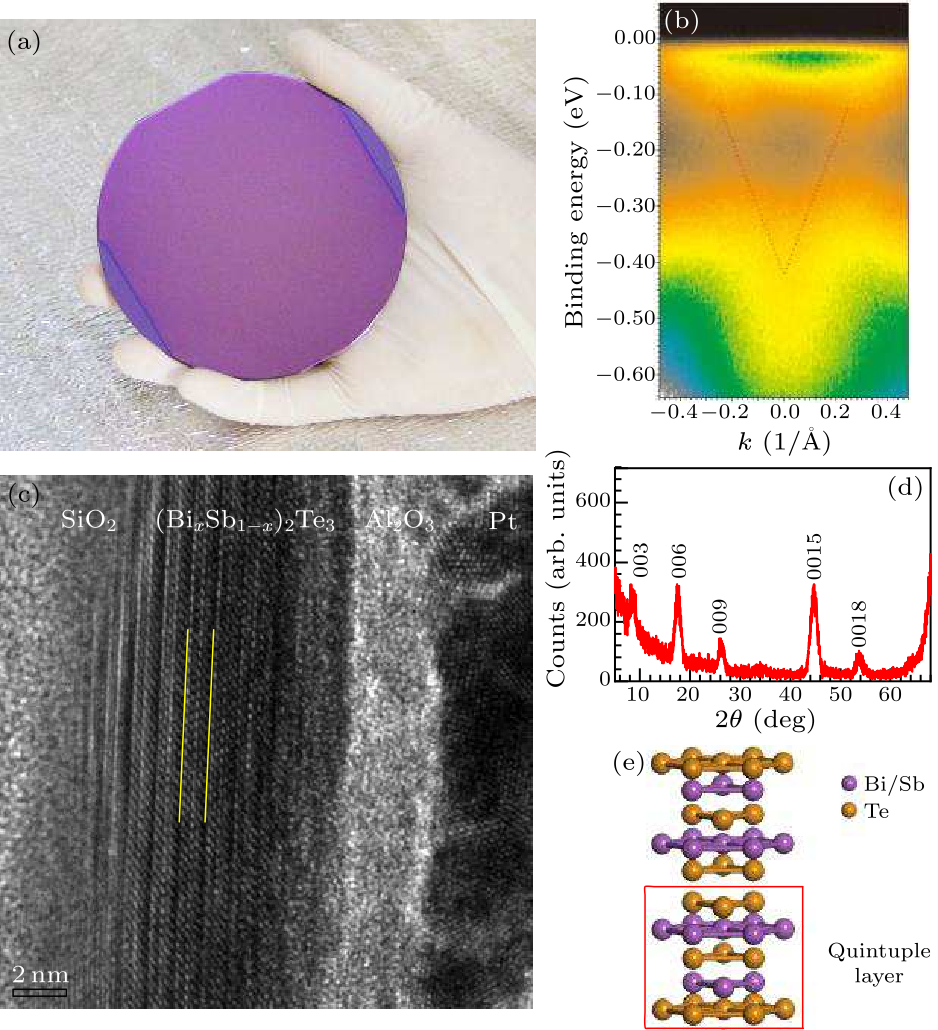
Fig. 1. Structural characterization of Bi$_{2}$Te$_{3}$ and BST thin films grown on amorphous SiO$_{2}$/Si by magnetron sputtering. (a) Photograph of a Bi$_{2}$Te$_{3}$/SiO$_{2}$ film with a diameter of 10 cm. (b) Electronic band structure of a Bi$_{2}$Te$_{3}$ thin film measured by ARPES showing linear dispersion of topological surface states (red dashed line). (c) HRTEM image and (d) XRD pattern of a BST thin film grown on amorphous SiO$_{2}$ (sample BST2). (e) The rhombohedral crystal structures of Bi$_{2}$Te$_{3}$ and (Bi$_{1-x}$Sb$_{x})_{2}$Te$_{3}$.
We grew (Bi$_{1-x}$Sb$_{x})_{2}$Te$_{3}$ films by cosputtering Bi$_{2}$Te$_{3}$ and Sb$_{2}$Te$_{3}$ alloy targets as well as Te targets on amorphous SiO$_{2}$/Si(100) substrates, which were kept at 160 $^{\circ}\!$C during growth. By modifying the Bi/Sb ratio in the films, one can control the density as well as the type of carriers in the films. The Bi/Sb ratio in the films was controlled by the sputtering powers of the Bi$_{2}$Te$_{3}$ and Sb$_{2}$Te$_{3}$ target guns. The Te target was also turned on at the same time to reduce the Te deficiency in the films. After growth, the films were annealed at 160 $^{\circ}\!$C for 25 min. Figure 1(a) shows a photograph of a 10 cm (4 inch) diameter silicon wafer with a 10 nm thick Bi$_{2}$Te$_{3}$ film grown on it, which maintains uniform properties across the whole film. Figure 1(c) displays a high-resolution transmission electron microscopy (HRTEM) cross-sectional image of a (Bi$_{1-x}$Sb$_{x})_{2}$Te$_{3}$ film, which shows the characteristic quintuple-layer structure of Bi$_{2}$Te$_{3}$. Although the film is polycrystalline, all the grains have the same $c$ orientation (normal to the cleavage plane). The crystalline structure of the BST film was further confirmed by x-ray diffraction (XRD) measurements (Fig. 1(d)). The presence of only ($0, 0, 3n$) diffraction peaks suggests that the film plane is parallel to the cleavage plane. This postulation is reasonable because the material has a layered structure, which means that the cleavage surface has a quite low surface free energy. The above structural characterization results demonstrate that we can indeed obtain Bi$_{2}$Te$_{3}$ family TI films with decent crystalline quality via magnetron sputtering. We used ARPES to assess the electronic band structure of a 10 QL-thick Bi$_{2}$Te$_{3}$ film grown by magnetron sputtering. Although the film is composed of domains of various in-plane crystalline orientations, the different domains have similar surface state band dispersion near the Dirac point because of the isotropy of the topological surface states around here, which will give observable ARPES signals. We indeed identified energy bands with similar band dispersion to the topological surface states of Bi$_{2}$Te$_{3}$ (Fig. 1(b)). The observation further confirms that we obtained Bi$_{2}$Te$_{3}$ TI films with magnetron sputtering, although the randomly orientated grains can significantly broaden the spectra. For transport studies, we prepared three (Bi$_{1-x}$Sb$_{x})_{2}$Te$_{3}$ samples, BST1, BST2 and BST3, with $x = 0.74$, 0.72 and 0.58, respectively. Figure 2(b) shows the $R_{xx}$–$T$ curve of the BST2 film. At high temperatures (in the region of $\sim $88–300 K), $R_{xx}$ increases with increasing $T$, showing semiconductor-like behavior and indicating that $E_{\rm F}$ is in the bulk band gap. The $R_{xx}$–$T$ curve displays metallic behavior in the intermediate temperature region ($\sim $7–88 K), which can be the result of reduced electron-phonon scattering of the surface states.[15,23,24] A second increase in $R_{xx}$ when $T$ is lower than 7 K can be ascribed to the electron-electron interaction to conduction, which is similar to those of the MBE-grown films of similar composition and thickness.[23–25] Moreover, Fig. 2(c) shows the Hall resistance of sample BST2 as a function of magnetic field $R_{xy}(\mu_{0}H)$ at various gate voltages. The $R_{xy}$–$\mu_{0}H$ curves are always linear over the entire range of the magnetic field ($\pm$2 T), and the positive slopes of $R_{xy}$–$\mu_{0}H$ as the gate voltage $V_{\rm g}$ increases from $-120$ V to $-15$ V suggest that the dominant carriers are p-type, while the negative slopes of $R_{xy}$–$\mu_{0}H$ as $V_{\rm g}$ continue to increase show that the dominant carriers are n-type. The zero-field longitudinal resistance $R_{xx}$ and Hall coefficient $R_{\rm H}$ extracted from $R_{xy}$–$\mu_{0}H$ curves of sample BST1-3 are plotted in Figs. 2(d)–2(f) as a function of gate voltage. In the case of BST1 (BST3), the $R_{xx}$ monotonically increases (decreases) with increasing $V_{\rm g}$, and the $R_{\rm H}$ has positive (negative) signs, indicating that BST1 (BST3) is a p-type (n-type) semiconductor. On the other hand, in sample BST2, when $V_{\rm g}$ is approximately 0 V, $R_{\rm H}$ reverses its sign, while $R_{xx}$ reaches its maximum value. These results clearly demonstrate the ambipolar field effect of Dirac dispersions and suggest that the Fermi level can be controlled across the DP by tuning the ratio of Bi to Sb (Fig. 2(a)) and back-gate voltages. We note that for sample BST2, the maximum value of $R_{xx}$, corresponding to the gate voltage at the charge neutral point, is on the same order as the maximum values of BST samples deposited by CVD or MBE, as listed in Table 1, and is also in the same order as the quantum resistance. The 2D carrier densities $n_{\rm 2D}=1/(eR_{\rm H})$ (where $e$ is the elementary charge) can be obtained from the linear ordinary Hall resistance, and the lowest carrier density is $n_{\rm 2D} = 2.7\times 10^{12}$ cm$^{-2}$ at $V_{\rm g}=60$ V with a corresponding mobility of 270 cm$^{2}$/Vs for electrons, while the lowest carrier density is $n_{\rm 2D} = 2.3\times 10^{12}$ cm$^{-2}$ at $V_{\rm g}= -120$ V with a corresponding mobility of 310 cm$^{2}$/Vs for holes. It can be concluded that magnetron sputtering is an effective method to prepare BST thin films with insulating bulk and low carrier densities, while the highly tunable Fermi level on SiO$_{2}$ allows us to explore the novel properties of topological surface states near the DP.
cpl-37-5-057301-fig2.png
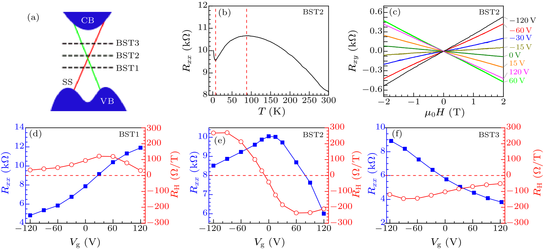
Fig. 2. Electrical transport in 7 nm thick BST thin films. (a) Schematic band structure for samples BST1, BST2 and BST3 and the corresponding Fermi levels, where CB, VB and SS are the bulk conduction band, bulk valance band and surface state, respectively. (b) The temperature ($T$) dependence of the longitudinal sheet resistance ($R_{xx}$) at zero magnetic field. From left to right, two red dashed lines are located at $T=7$ K and $T=88$ K, respectively. (c) Hall resistance $R_{xy}$ as a function of magnetic field $\mu_{0}H$ at 2 K tuned by the back-gate voltage. (d)–(f) Dependence of zero field longitudinal sheet resistance $R_{xx}$(0) (solid squares) and Hall coefficient $R_{\rm H}$ (open circles) on the back-gate voltage for samples BST1 (d), BST2 (e) and BST3 (f) at $T=2$ K.
Table 1. Gate-tuned longitudinal sheet resistance of BST samples developed by different techniques.
Device $R_{xx}$ (k$\Omega$) $T$ (K) Thickness
CVD-grown BST 0.5–5.5 2 5 nm Ref. [26]
MBE-grown BST 8–12 2.2 20 nm Ref. [27]
3–12 0.04 8 nm Ref. [28]
2–6 2.1 7 nm Ref. [29]
2–8 1.6 8 nm Ref. [29]
1–3 1.6 20 nm Ref. [24]
2–12 1.4 10 nm Ref. [30]
3–12 6.9 10 nm Ref. [31]
Sputter-deposited BST 6–10 2 7 nm This work
After the BST thin films with bulk insulating properties were successfully prepared, we focused on the Cr-doped TI thin films grown by magnetron sputtering to investigate the possibility of realizing long-range ferromagnetic order and tuning $E_{\rm F}$ inside the surface gap. One way to generate long-range ferromagnetic order in TIs is magnetic doping, and magnetically doped TI materials have been grown by CVD,[32] bulk Bridgman growth[33–36] and MBE.[37] Until now, however, magnetron sputtering has rarely been adopted for this purpose. In our experiment, CBST films were prepared by the cosputtering of Sb$_{2}$Te$_{3}$, Bi$_{2}$Te$_{3}$, Te and Cr targets at a substrate temperature of 175 $^{\circ}\!$C. Figure 3 presents an example of ferromagnetic properties observed in a 6 nm thick Cr$_{0.24}$(Bi$_{0.36}$Sb$_{0.64})_{1.76}$Te$_{3}$ film. At $T=2$ K, the conventional butterfly-shaped $R_{xx}-\mu_{0}H$ curve and nearly square-shaped Hall hysteresis loop with a coercive field of 340 Oe shown in Figs. 3(a) and 3(b) suggest that the long-range ferromagnetic order with perpendicular magnetic anisotropy is developed at low temperatures. A Curie temperature ($T_{\rm c}$) of 11 K is determined by an Arrott plot (Fig. 3(c)), in which $R_{xy}^{2}$ is plotted against $\mu_{0}H/R_{xy}$ and the extrapolated intercept is proportional to the saturation magnetization.
cpl-37-5-057301-fig3.png
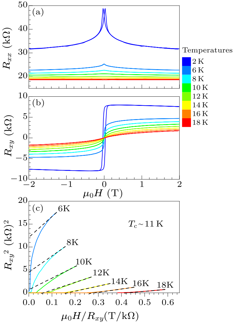
Fig. 3. Ferromagnetic characterization of a 6 nm thick CBST thin film. (a) Longitudinal resistance $R_{xx}$ and (b) Hall resistance $R_{xy}$ vs $\mu_{0}H$ at different temperatures. (c) Arrott plot of the CBST thin film.
Generally, the Hall resistance of the anomalous Hall effect is expressed as[37,38] $$ R_{xy}=R_{0}H + R_{\rm AH}(M),~~ \tag {1} $$ where $R_{0}$ is the slope of the ordinary Hall background, $H$ is the applied magnetic field, and $M$ is the magnetization component in the perpendicular direction. Figures 4(a) and 4(b) present the longitudinal sheet resistance $R_{xx}$ and Hall resistance $R_{xy}$, respectively, as a function of $H$ of a CBST thin film at various back-gate voltages. $R_{\rm AH}$ estimated by the intercept of the linear background at a high magnetic field and zero field $R_{xx}(0)$ are plotted in Fig. 4(c). We observe that the $R_{\rm AH}$ and $R_{xx}(0)$ data point towards the same trend and both reach their maxima at $V_{\rm g}= -130$ V and their minima at $V_{\rm g}=150$ V. It is worth noting that the maximum of $R_{\rm AH}$ in Fig. 4(c) is 16.4 k$\Omega$, which exceeds 60% of the quantum Hall resistance ($h/e^{2}$). More importantly, the existence of robust ferromagnetic order in both p-type and n-type Cr-doped TI thin films grown by magnetron sputtering and the $V_{\rm g}$-independent coercive field shown in Fig. 4(b) demonstrate the occurrence of carrier-independent bulk van Vleck magnetism, which is consistent with the results reported in the literature.[37,39]
cpl-37-5-057301-fig4.png
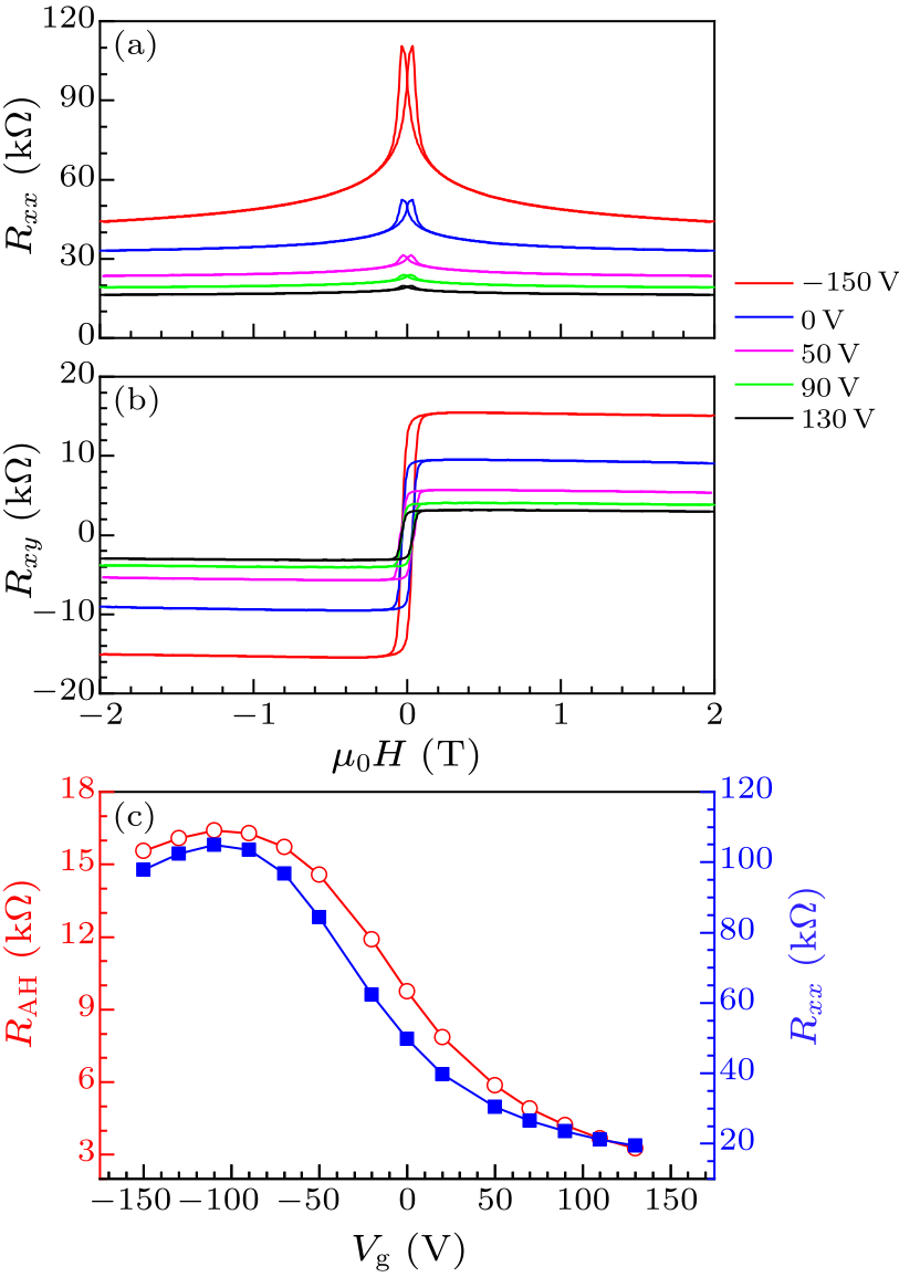
Fig. 4. (a) Longitudinal sheet resistance $R_{xx}$ and (b) Hall resistance $R_{xy}$ vs $\mu_{0}H$ at different gate voltages at a temperature of 2 K. (c) $V_{\rm g}$-dependent $R_{\rm AH}$ (open circles) and $R_{xx}$(0) (solid squares) measured at 2 K.
Nevertheless, the QAHE has not been observed in our Cr-doped TI films grown by magnetron sputtering. In the quantum anomalous Hall regime, $R_{\rm AH}$ should reach a maximum, and $R_{xx}$ should exhibit a dip at the charge neutral point.[20,40,41] This signature has not been observed in our CBST thin films at $T= 2$ K. The $R_{\rm AH}/R_{xx}(0)$ ratio of the CBST thin film, however, has a maximum of approximately 0.2 at $V_{\rm g}=20$ V (see Fig. S6 in the Supplementary Materials), which exceeds the Hall angle of usual diluted magnetic semiconductors.[37] Therefore, the quantum anomalous edge states in CBST may contribute to carrier transport. We believe that it will be possible to observe the QAHE at 2 K or lower temperature in CBST thin films grown by magnetron sputtering if the quality of the sample is improved further by reducing the sputtering rate, controlling the amount of Cr more precisely and adjusting the annealing process, among other measures. In summary, we have demonstrated that it is possible to grow Bi$_{2}$Te$_{3}$ family TI thin films on amorphous SiO$_{2}$/Si substrates by magnetron sputtering. Our work provides a large-scale method to produce bulk insulating TI thin films with tunable transport properties. Both the ARPES data and the ambipolar field effect point to the conclusion that the topological surface states can very well exist in these sputtered polycrystalline thin films. An unusually large value of 60% of the quantum anomalous Hall resistance is observed in Cr-doped BST films, and more efforts are needed to obtain an ideal quantum anomalous Hall insulator. The magnetron cosputtering growth provides a first yet important step towards the large-scale fabrication of multilayer films with complex structures for future spintronic devices. Magnetron sputtering growth.—Bi$_{2}$Te$_{3}$, BST and CBST thin films were grown on polished, thermally oxidized silicon substrates (300 nm SiO$_{2}$/silicon) by magnetron sputtering. The cosputtering method with a high-purity (99.99%) Bi$_{2}$Te$_{3}$ alloying target, Sb$_{2}$Te$_{3}$ alloying target and Te target was adopted to control the films' composition. The BST thin films were deposited from Bi$_{2}$Te$_{3}$ and Sb$_{2}$Te$_{3}$ targets by dc sputtering and from a Te target by rf sputtering. The CBST thin films were deposited from Bi$_{2}$Te$_{3}$, Sb$_{2}$Te$_{3}$ and Cr (99.95%) targets by dc sputtering and a Te target by rf sputtering. During growth, the Si(100) substrate was kept at 160 $^{\circ}\!$C for BST thin films and at 175 $^{\circ}\!$C for CBST thin films. The base pressure of the deposition chamber was below $3\times 10^{-7}$ Torr, and the working argon pressure was set at $2\times 10^{-3}$ Torr. After growth, the thin films were annealed for 25 min at the same temperature as the deposition. When the substrate temperature was cooled to room temperature, a 3–4 nm thick Al thin film was sputtered in situ on the topological insulator thin films, and the Al thin film was naturally oxidized to form Al$_{2}$O$_{3}$ after the sample was removed from the chamber and exposed in air. Material characterization.—To avoid possible contamination of Bi$_{2}$Te$_{3}$ thin films, a 2 nm thick Te capping layer was deposited on top of the films before we removed them from the high-vacuum growth chamber. The Bi$_{2}$Te$_{3}$ thin films with a 2 nm Te capping layer were exposed in air for two hours before ARPES measurements. ARPES data were collected by a Scienta R4000 analyzer at a 3 K sample temperature. The Sb, Bi and Cr concentrations in the films were determined by using inductively coupled plasma atomic emission spectroscopy (ICP-AES). The structural characteristics of BST films were investigated by using TEM (FEI Tecnai F20; acceleration voltage, 200 kV) and XRD (Rigaku TTR-III, Japan). Transport measurement.—The Bi$_{2}$Te$_{3}$, BST and CBST thin films were mechanically scratched into six-terminal Hall bar configurations by a sharp metal tip; then, aluminum wires were glued to each terminal with silver epoxy to form ohmic contacts. The $R_{xx}$ and $R_{xy}$ data were symmetrized and antisymmetrized, respectively, to account for the misalignment of electrodes. The transport measurements were carried out using a 9 T Physical Properties Measurement System (PPMS, Quantum Design) with a base temperature of 2 K.
References Colloquium : Topological insulatorsThe quantum spin Hall effect and topological insulatorsMagnetization switching through giant spin–orbit torque in a magnetically doped topological insulator heterostructureElectric-field control of spin–orbit torque in a magnetically doped topological insulatorCurrent-Nonlinear Hall Effect and Spin-Orbit Torque Magnetization Switching in a Magnetic Topological InsulatorRoom-Temperature Spin-Orbit Torque Switching Induced by a Topological InsulatorRoom-temperature high spin–orbit torque due to quantum confinement in sputtered BixSe(1–x) filmsTopological Transitions Induced by Antiferromagnetism in a Thin-Film Topological InsulatorRoom temperature magnetization switching in topological insulator-ferromagnet heterostructures by spin-orbit torquesTailoring exchange couplings in magnetic topological-insulator/antiferromagnet heterostructuresA magnetic heterostructure of topological insulators as a candidate for an axion insulatorTopological antiferromagnetic spintronicsExperimental Realization of a Three-Dimensional Topological Insulator, Bi2Te3Observation of a large-gap topological-insulator class with a single Dirac cone on the surfaceBulk Band Gap and Surface State Conduction Observed in Voltage-Tuned Crystals of the Topological Insulator Bi 2 Se 3 Aharonov–Bohm interference in topological insulator nanoribbonsGranularity Controlled Nonsaturating Linear Magnetoresistance in Topological Insulator Bi 2 Te 3 FilmsMolecular Beam Epitaxial Growth of Topological InsulatorsAchieving Surface Quantum Oscillations in Topological Insulator Thin Films of Bi 2 Se 3Experimental Observation of the Quantum Anomalous Hall Effect in a Magnetic Topological InsulatorThickness-dependent transport channels in topological insulator Bi2Se3 thin films grown by magnetron sputteringBulk transport properties of bismuth selenide thin films grown by magnetron sputtering approaching the two-dimensional limitEvidence for electron-electron interaction in topological insulator thin filmsHighly tunable electron transport in epitaxial topological insulator (Bi 1- x Sb x ) 2 Te 3 thin filmsTrajectory of the anomalous Hall effect towards the quantized state in a ferromagnetic topological insulatorAmbipolar field effect in the ternary topological insulator (BixSb1–x)2Te3 by composition tuningGate control of surface transport in MBE-grown topological insulator (Bi 1 x Sb x ) 2 Te 3 thin filmsQuantum Hall effect on top and bottom surface states of topological insulator (Bi1−xSbx)2Te3 filmsMapping the chemical potential dependence of current-induced spin polarization in a topological insulatorQuantum and Classical Magnetoresistance in Ambipolar Topological Insulator Transistors with Gate-tunable Bulk and Surface ConductionBulk-impurity induced noise in large-area epitaxial thin films of topological insulatorsMagnetic Doping and Kondo Effect in Bi 2 Se 3 NanoribbonsDevelopment of ferromagnetism in the doped topological insulator Bi 2 x Mn x Te 3 Dirac-fermion-mediated ferromagnetism in a topological insulatorCarriers dependence of the magnetic properties in magnetic topological insulator Sb1.95−xBixCr0.05Te3Carrier dependent ferromagnetism in chromium doped topological insulator Cry(BixSb1x)2yTe3Thin Films of Magnetically Doped Topological Insulator with Carrier-Independent Long-Range Ferromagnetic OrderAnomalous Hall effectInterplay between Different Magnetisms in Cr-Doped Topological InsulatorsHigh-precision realization of robust quantum anomalous Hall state in a hard ferromagnetic topological insulatorGiant anisotropic magnetoresistance in a quantum anomalous Hall insulator
[1] Hasan M Z and Kane C L 2010 Rev. Mod. Phys. 82 3045
[2] Qi X L and Zhang S C 2010 Phys. Today 63 33
[3] Fan Y B et al 2014 Nat. Mater. 13 699
[4] Fan Y B et al 2016 Nat. Nanotechnol. 11 352
[5] Yasuda K et al 2017 Phys. Rev. Lett. 119 137204
[6] Han J H et al 2017 Phys. Rev. Lett. 119 077702
[7] Dc M et al 2018 Nat. Mater. 17 800
[8] He Q L et al 2018 Phys. Rev. Lett. 121 096802
[9] Wang Y et al 2017 Nat. Commun. 8 1364
[10] He Q L et al 2017 Nat. Mater. 16 94
[11] Mogi M et al 2017 Nat. Mater. 16 516
[12] Šmejkal L et al 2018 Nat. Phys. 14 242
[13] Chen Y L et al 2009 Science 325 178
[14] Xia Y et al 2009 Nat. Phys. 5 398
[15] Checkelsky J G et al 2011 Phys. Rev. Lett. 106 196801
[16] Peng H et al 2010 Nat. Mater. 9 225
[17] Wang Z H, Yang L, Li X J, Zhao X T, Wang H L, Zhang Z D and Gao X P 2014 Nano Lett. 14 6510
[18] Chen X, Ma X C, He K, Jia J F and Xue Q K 2011 Adv. Mater. 23 1162
[19] Taskin A A, Sasaki S, Segawa K and Ando Y 2012 Adv. Mater. 24 5581
[20] Chang C Z, Zhang J S, Feng X, Shen J, Zhang Z C, Guo M H, Li K, Ou Y B, Wei P, Wang L L, Ji Z Q, Feng Y, Ji S H, Chen X, Jia J F, Dai X, Fang Z, Zhang S C, He K, Wang Y Y, Lu L, Ma X C and Xue Q K 2013 Science 340 167
[21] Wang W J, Gao K H and Li Z Q 2016 Sci. Rep. 6 25291
[22] Sapkota Y R and Mazumdar D 2018 J. Appl. Phys. 124 105306
[23] Wang J, DaSilva A M, Chang C Z, He K, Jain J K, Samarth N, Ma X C, Xue Q K and Chan M H W 2011 Phys. Rev. B 83 245438
[24] He X Y, Guan T, Wang X X, Feng B J, Cheng P, Chen L, Li Y Q and Wu K H 2012 Appl. Phys. Lett. 101 123111
[25] Checkelsky J G, Yoshimi R, Tsukazaki A, Takahashi K S and Tokura Y 2014 Nat. Phys. 10 731
[26] Kong D S, Chen Y L, Cha J J, Zhang Q F, Analytis J G, Lai K J, Liu Z K, Hong S S, Koski K J and Mo S K 2011 Nat. Nanotechnol. 6 705
[27] Shimizu S, Yoshimi R, Hatano T, Takahashi K S, Tsukazaki A, Kawasaki M, Iwasa Y and Tokura Y 2012 Phys. Rev. B 86 045319
[28] Yoshimi R, Tsukazaki A, Kozuka Y, Falson J, Takahashi K S, Checkelsky J G, Nagaosa N, Kawasaki M and Tokura Y 2015 Nat. Commun. 6 6627
[29] Lee J S, Richardella A, Hickey D R, Mkhoyan K A and Samarth N 2015 Phys. Rev. B 92 155312
[30] Tian J F, Chang C Z, Cao H L, He K, Ma X C, Xue Q K and Chen Y P 2015 Sci. Rep. 4 4859
[31] Islam S, Bhattacharyya S, Kandala A, Richardella A, Samarth N and Ghosh A 2017 Appl. Phys. Lett. 111 062107
[32] Cha J J, Williams J R, Kong D, Meister S, Peng H, Bestwick A J, Gallagher P, Goldhaber G D and Cui Y 2010 Nano Lett. 10 1076
[33] Hor Y S, Roushan P, Beidenkopf H, Seo J, Qu D, Checkelsky J G, Wray L A, Hsieh D, Xia Y, Xu S Y, Qian D, Hasan M Z, Ong N P, Yazdani A and Cava R J 2010 Phys. Rev. B 81 195203
[34] Checkelsky J G, Ye J T, Onose Y, Iwasa Y and Tokura Y 2012 Nat. Phys. 8 729
[35] Li H, Song Y R, Yao M Y, Yang F, Miao L, Zhu F F, Liu C H, Gao C L, Qian D, Yao X, Jia J F, Shi Y J and Wu D 2012 Appl. Phys. Lett. 101 072406
[36] Li B, Fan Q Y, Ji F H, Liu Z, Pan H and Qiao S 2013 Phys. Lett. A 377 1925
[37] Chang C Z, Zhang J S, Liu M H, Zhang Z C, Feng X, Li K, Wang L L, Chen X, Dai X and Fang Z 2013 Adv. Mater. 25 1065
[38] Nagaosa N, Sinova J, Onoda S, MacDonald A H and Ong N P 2010 Rev. Mod. Phys. 82 1539
[39] Kou X F, Lang M R, Fan Y B, Jiang Y, Nie T X, Zhang J M, Jiang W J, Wang Y, Yao Y G, He L and Wang K L 2013 ACS Nano 7 9205
[40] Chang C Z, Zhao W, Kim D Y, Zhang H J, Assaf B A, Heiman D, Zhang S C, Liu C X, Chan M H W and Moodera J S 2015 Nat. Mater. 14 473
[41] Kandala A, Richardella A, Kempinger S, Liu C X and Samarth N 2015 Nat. Commun. 6 7434