Chinese Physics Letters, 2019, Vol. 36, No. 7, Article code 078501 A New Effect of Oxygen Plasma on Two-Dimensional Field-Effect Transistors: Plasma Induced Ion Gating and Synaptic Behavior * Cheng-Lei Guo (郭成磊)1,2,3, Bin-Bin Wang (王斌斌)2, Wei Xia (夏威)2, Yan-Feng Guo (郭艳峰)2, Jia-Min Xue (薛加民)2** Affiliations 1Shanghai Institute of Optics and Fine Mechanics, Chinese Academy of Sciences, Shanghai 201800 2School of Physical Science and Technology, ShanghaiTech University, Shanghai 201210 3Center of Materials Science and Optoelectronics Engineering, University of Chinese Academy of Sciences, Beijing 100049 Received 12 February 2019, online 20 June 2019 *Supported by the National Key Research and Development Program of China under Grant No 2017YFA0305400, the ShanghaiTech University, and the Natural Science Foundation of Shanghai under Grant No 17ZR1443300.
**Corresponding author. Email: xuejm@shanghaitech.edu.cn
Citation Text: Guo C L, Wang B B, Xia W, Guo Y F and Xue J M et al 2019 Chin. Phys. Lett. 36 078501    Abstract Plasma treatment is a powerful tool to tune the properties of two-dimensional materials. Previous studies have utilized various plasma treatments on two-dimensional materials. We find a new effect of plasma treatment. After controlled oxygen-plasma treatment on field-effect transistors based on two-dimensional SnSe$_{2}$, the capacitive coupling between the silicon back gate and the channel through the 300 nm SiO$_{2}$ dielectric can be dramatically enhanced by about two orders of magnitude (from 11 nF/cm$^{2}$ to 880 nF/cm$^{2}$), reaching good efficiency of ion-liquid gating. At the same time, plasma treated devices show large hysteresis in the gate sweep demonstrating memory behavior. We reveal that this spontaneous ion gating and hysteresis are achieved with the assistance of a thin layer of water film automatically formed on the sample surface with water molecules from the ambient air, due to the change in hydrophilicity of the plasma treated samples. The water film acts as the ion liquid to couple the back gate and the channel. Thanks to the rich carrier dynamics in plasma-treated two-dimensional transistors, synaptic functions are realized to demonstrate short- and long-term memories in a single device. This work provides a new perspective on the effects of plasma treatment and a facile route for realizing neuromorphic devices. DOI:10.1088/0256-307X/36/7/078501 PACS:85.30.Tv, 52.77.-j, 73.50.-h © 2019 Chinese Physics Society Article Text Few-layer two-dimensional (2D) materials have ultimate surface-to-volume ratios which can offer a large freedom of tunability for device functions. Treating the surface alone can significantly modify the devices after fabrication, which is not achievable for traditional devices based on bulk materials such as Si. For example, deposition of various materials on top of 2D channels can greatly influence the mobility,[1,2] doping type,[3,4] band gap[5] and so on. Plasma treatment is an equally powerful technique. High energy ions or radicals in the plasma can have multiple effects on 2D materials. Physically the ion bombardments can knock out atoms of the top layers and can control the thickness of the 2D channel. Very uniform and precise thinning has been obtained on MoS$_{2}$,[6] ReS$_{2}$,[7] black phosphorus[8] and so on, by O$_{2}$ or Ar plasma. On the other hand, the radicals in the plasma can introduce doping species or defects into the 2D lattice, thus changing the doping type and forming p–n junctions in the channel.[4,7] When a large amount of atomic defects are introduced, even phase transition can be triggered in 2D materials with multiple phases.[9] After enough reaction with the plasma, the surface layers of some 2D materials (such as black phosphorus) can be completely converted to other amorphous materials (such as PO$_{x}$),[10] providing a capping layer for air sensitive channel materials underneath. All these previous studies establish plasma treatment as a versatile tool for tuning the properties of 2D materials and devices. In this work, we unveil a new effect associated with plasma treatment. We use field-effect transistors (FETs) based on a 2D material SnSe$_{2}$ as a model system, and reveal that after controlled oxygen plasma treatment the capacitive coupling between the silicon back gate and the channel can increase by about two orders of magnitude. At the same time, large hysteresis (memory effect) in the gate sweeping emerges. Surprisingly, this behavior will completely disappear if we measure the transport in vacuum or in dry air, and can recover as soon as the device is exposed to ambient air. By performing water contact angle and Hall measurements, we reveal this effect as a result of water film forming on the plasma treated devices and automatic ionic gating through capacitive coupling between the water film and the silicon back gate. Due to the slow dynamics of ions in water and trap states introduced to the channel through plasma, we can mimic the synaptic behavior and realize both the short-term and long-term memories in a single type of plasma treated devices. These findings provide new insights into the plasma treatment of 2D materials and demonstrate a facile route for achieving neuromorphic effects in FETs. The SnSe$_{2}$ device fabrication starts with Scotch tape exfoliation of thin SnSe$_{2}$ flakes on heavily doped silicon wafer covered with 300-nm-thick SiO$_{2}$ as the back-gate dielectric. Standard electron-beam lithography and metal deposition (5 nm Ti and 50 nm Au) were utilized to fabricate the SnSe$_{2}$ FET devices. Figure 1(a) shows the schematic of the device. As previously reported,[11,12] SnSe$_{2}$ FETs on 300 nm SiO$_{2}$ are very difficult to be fully depleted at room temperature with the back gate only, due to its intrinsic high electron-doping level of $\sim$$10^{19}$ cm$^{-3}$. The transfer measurement of a 17.7-nm-thick SnSe$_{2}$ in Fig. 1(b) (black curve) confirms this property. The gate voltage linearly modulates the conductance of the device in the sweep from $-20$ V to 20 V, with a small conductance change of about 20%. By extrapolating the curve to zero conductance, we can obtain an estimate of the threshold voltage to be about $-$190 V, approaching the dielectric breakdown voltage of the 300 nm SiO$_{2}$. To explore the possible doping effect of electron plasma[13–15] to reduce the carrier density, we expose the device to mild O$_{2}$ plasma for 15 s (see the Supplementary Material (SM) for details). If the only effect of the plasma treatment was the reduction of carrier density, we would expect the black transfer curve in Fig. 1(b) to parallel shift down. However, what we actually obtain is greatly enhanced gate tunability and a large gate hysteresis, as shown by the red curve in Fig. 1(b). Some other devices show an even more dramatic change, and the conductance modulation by the gate sweep can be increased from order one to 10$^{3}$ (see Fig. S1 in the SM). Conventionally, the slope of the transfer curve is used to extract the carrier mobility $\mu$, since $\mu=\frac{L}{W}\times(dG_{\rm ds}/dV_{\rm g})/C_{\rm ox}$, where $L$ ($W$) is the length (width) of the channel, $G_{\rm ds}$ is the conductance, $V_{\rm g}$ is the gate voltage, and $C_{\rm ox}$ is the specific capacitance of the 300 nm SiO$_{2}$. The great change of slopes near zero gate voltage in Fig. 1(b) from the black curve (before plasma) to the red curve (after plasma) appears to indicate that the mobility has been enhanced by more than one order of magnitude. This surprising result contradicts the expectation that mobility would in general go down with plasma treatment since more defects are introduced to the channel.[15] One possibility is that after reaction with O$_{2}$ plasma, the channel has changed from SnSe$_{2}$ to a new material with very high mobility. To check this possibility, Raman spectroscopy is used to measure the characteristic phonon modes of SnSe$_{2}$. We can see that after plasma treatment, the SnSe$_{2}$ Raman peaks show no shift or change of width, indicating that the channel still consists mostly of intact SnSe$_{2}$ lattices. The small Raman peak near 250 cm$^{-1}$ can be attributed to amorphous Se,[16] presumably resulting from the replacement of some Se atoms by O atoms in the lattices (corroborated by the x-ray photoelectron spectroscopy (XPS) results of plasma treated bulk SnSe$_{2}$ in Fig. S2 of the SM). Atomic force microscopy (AFM) is also used to measure the thickness and surface roughness of the device in Fig. 1(b). A thickness increase of 1.3 nm is in accordance with the production of the amorphous Se layer on the surface. On the other hand, a reduction of roughness from 0.8 nm to 0.4 nm probably comes from the cleaning of surface residues by O$_{2}$ plasma. These results indicate that the greatly enhanced slope in the transfer curves is unlikely due to a conversion of the channel from SnSe$_{2} $ to another high-mobility material.
cpl-36-7-078501-fig1.png
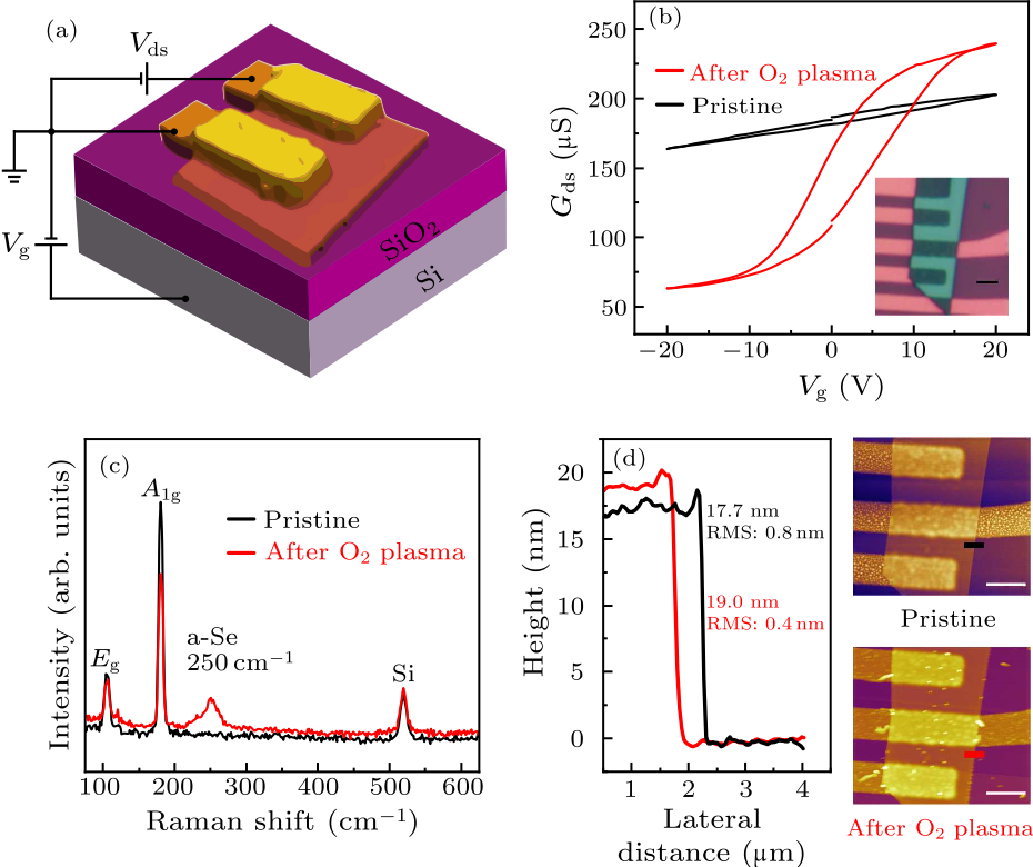
Fig. 1. Basic characterizations of the SnSe$_{2}$ FETs before and after plasma treatment. (a) Schematic of the SnSe$_{2}$ thin flake FET device. (b) Conductance versus gate voltage for a typical SnSe$_{2}$ FET device in air before (black) and after (red) oxygen plasma treatment. Inset: the optical microscope image of the device. The scale bar is 10 µm. (c) Raman spectra of a SnSe$_{2}$ flake before (black) and after (red) oxygen plasma treatment. (d) AFM measurements before (black) and after (red) oxygen plasma treatment of the device shown in (b). The scale bars are 10 µm.
More interestingly, we find that the great enhancements of the transfer-curve slope and hysteresis are very sensitive to the measurement condition. Figure 2(a) shows the transfer curves of another plasma treated SnSe$_{2}$ device. Usually the time interval before each measurement is about 1 h. We expose the plasma treated device to a specific condition for 0.5 h before test. When measured in ambient air, the device demonstrates the large gate tunability and hysteresis (red solid line). However, when the device is measured in vacuum ($\sim$$5\times 10^{-3}$ Pa), the slope of the transfer curve decreases by one order of magnitude (black filled circles) and no hysteresis can be seen. To find out which component of the air contributes to this behavior, we vent the vacuum chamber with pure O$_{2}$, N$_{2}$ and even desiccated ambient air (see Fig. S3 in the SM for details), and the transfer curve remains the same (red filled triangles are data with dry air). Only when we vent the vacuum chamber with unprocessed ambient air could the large slope and hysteresis of the transfer curve be recovered (black solid line). Thus we identify the critical role played by the water moisture in air in causing the great enhancement of gate tunability and hysteresis of SnSe$_{2}$ devices.
cpl-36-7-078501-fig2.png
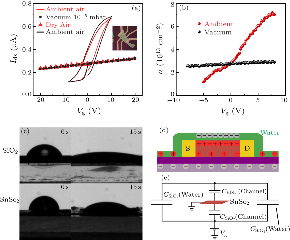
Fig. 2. Unveiling the mechanism of greatly enhanced coupling between the gate and channel. (a) Transfer measurements under different conditions showing the important role of water. The relative humidity of ambient air is 60%. The inset shows the optical microscope image of the device. (b) Hall measurements of the carrier density as a function of gate voltage under vacuum and ambient conditions. (c) Water contact angles, indicating that the hydrophilicity has increased for both SiO$_{2}$ and SnSe$_{2}$ after O$_{2}$ plasma treatment. (d) The model to explain the greatly enhanced capacitive coupling between the back gate and the channel. A water film (green colored layer) is formed on the whole sample to act as an ion liquid. (e) The equivalent capacitance circuit to calculate the effective capacitive coupling between the gate and the channel.
However, what role does water moisture play in this process? Does it help to greatly enhance the channel mobility? To clarify these issues, Hall measurements of the device in ambient air and in vacuum are adopted (see the SM for measurement details). As shown in Fig. 2(b), for a gate voltage sweep in vacuum from 0 V to 8 V, carriers of $2.3\times 10^{12}$ cm$^{-2}$ are induced. However, when we vent the Hall measurement chamber with ambient air, the same gate voltage sweep induces $4.4\times 10^{13}$ cm$^{-2}$ of carriers, more than one-order-of-magnitude higher. This astonishing result reveals that water moisture helps to greatly increase the capacitive coupling between the back gate and the channel. The extracted specific capacitance between the back gate and the channel is 880 nF/cm$^{2}$, much higher than $\sim 11.5$ nF/cm$^{2}$ provided by a 300 nm SiO$_{2}$ dielectric layer and approaching the value of the electron double layer (EDL) formed at the ion liquid and 2D semiconductor interface.[17–19] We then explain the greatly enhanced gate tenability and hysteresis of plasma treated SnSe$_{2}$ FETs based on the model shown in Fig. 2(d). A thin and continuous water film (the top green layer in the schematic) is automatically formed on the plasma treated devices in ambient air. Water contact angle measurements in Fig. 2(c) has confirmed that the hydrophilicity is greatly increased on both the SiO$_{2}$ and the SnSe$_{2}$ surfaces, presumably due to the dangling bonds formed on the surface after O$_{2}$ plasma treatment. This water film behaves as an ion liquid and significantly enhances the capacitive coupling between the back gate and the channel. When a negative voltage is applied to the gate as shown in Fig. 2(d), the bottom of the channel accumulates positive charges due to the conventional direct coupling through the SiO$_{2}$ dielectric. On the other hand, the rest of the gate (with the sample size of 1 cm$\times 1$ cm) couples with the water. Through ion movements, an EDL will be formed between the water film and the channel, and a large number of positive charges are induced on the top of the channel. Hence, a great modulation of the channel conductance is achieved. The equivalent capacitance circuit is drawn in Fig. 2(e) to quantitatively describe this process. The total capacitance between the back gate and the channel is $$\begin{align} C_{\rm total} =\,&C_{{\rm SiO}_{2}} ({\rm channel})\\ &+\frac{C_{{\rm SiO}_{2}} ( {\rm water})C_{\rm EDL} ({\rm channel})}{C_{{\rm SiO}_{2}} ({\rm water})+C_{\rm EDL} ({\rm channel})}, \end{align} $$ where $C_{{\rm SiO}_{2}} ({\rm channel})$ is the capacitance between the gate and the channel through the 300 nm SiO$_{2}$, $C_{{\rm SiO}_{2}} ({\rm water})$ is the capacitance between the gate and the water film through the 300 nm SiO$_{2}$, and $C_{\rm EDL}({\rm channel})$ is the capacitance of the EDL. Since the area between the back gate and the water film is in the order of 1 cm$^{2}$, while that of the device is about 10 µm$^{2}$, $C_{{\rm SiO}_{2}} ({\rm water})$ is several orders of magnitude larger than $C_{{\rm SiO}_{2}} ( {\rm channel})$ and $C_{\rm EDL} ({\rm channel})$. Thus we have $$ C_{\rm total} \approx C_{{\rm SiO}_{2}} ({\rm channel})+C_{\rm EDL} ({\rm channel}). $$ A previous study measured the specific capacitance of the EDL between ion liquid and 2D materials to be around 1 µF/cm$^{2}$,[19] much higher than that of the 300 nm SiO$_{2}$ dielectric ($\sim$11.5 nF/cm$^{2}$). Then we obtain $C_{\rm total} \approx C_{\rm EDL} ({\rm channel})\approx 1$ µF/cm$^{2}$, which agrees well with our value extracted from the Hall measurement (880 nF/cm$^{2}$). The other feature of plasma treated FETs is the emergence of large hysteresis. This behavior can also be explained by the model in Fig. 2(d). Numerous studies have shown that ion gating has large hysteresis due to the slow movement of ions.[20–23] Although it is not good for conventional FET operation, this hysteresis can be exploited to realize a rich synaptic behavior. Short-term and long-term memories can both be realized based on this automatically formed ion gating of plasma treated FETs. To mimic a synapsis, the gate is used as the presynaptic input terminal and the O$_{2}$ plasma treated SnSe$_{2}$ channel with source/drain electrodes is used as the postsynaptic output terminal. We apply a voltage pulse to the gate and track the time evolution of the change of the source/drain current $\Delta I_{\rm ds}$. As shown in Fig. 3(a), for pristine devices, $\Delta I_{\rm ds}$ nicely follows the rising and falling edges of the gate pulse. However, after plasma treatment the falling edge of $\Delta I_{\rm ds}$ shows a prolonged decaying tail, mimicking the short-term synaptic plasticity in biological synapsis.[24,25] Such a decay behavior can be fitted by a stretched exponential function[26,27] $$ \Delta I_{\rm ds} ={\alpha}\exp \Big[-\Big({\frac{t-t_{0}}{\tau}}\Big)^{\beta}\Big], $$ where $\tau$ is the retention time, $t_{0}$ is the time when the pulse finishes, $\beta$ is the stretch index ranging between 0 and 1, and $\alpha$ is a proportional constant. The inset of Fig. 2(b) shows the fitted curve of the decaying $\Delta I_{\rm ds}$ and $\tau$ is extracted to be $\sim$0.18 s. Compared with short-term memories, long-term memories are more important for learning in biological systems.[28] It is usually difficult to realize both of them in a single type of neuromorphic device due to ion gating.[25] Remarkably, they can be achieved in the plasma-treated SnSe$_{2}$ FETs. As shown in Fig. 3(c), when a negative pulse is applied to the gate, initially $\Delta I_{\rm ds}$ follows the pulse wave form closely. A dramatic response happens right after the gate pulse is removed. Instead of returning to zero, $\Delta I_{\rm ds}$ increases to a much higher level and then decays with a time constant of $\sim $4 s, more than one order of magnitude longer than that of the short-term memory induced by a positive gate pulse. Even after 20 s, $I_{\rm ds}$ still remembers the negative pulse event ($\Delta I_{\rm ds} =47.5$ nA). We can understand these interesting results by considering the rich charge-carrier dynamics in the plasma treated SnSe$_{2}$ FETs. When a negative gate pulse is applied, electrons are repelled from the heavily n-doped channel through both the direct SiO$_{2}$ coupling and the water film EDL, and $I_{\rm ds}$ changes by $\Delta I_{\rm ds}$. This can be expressed as $$ \Delta I_{\rm ds}=\Delta ne\nu W, $$ where $\Delta n$ is the change of electron density, $e$ is the elemental charge, $\nu$ is the electron drift velocity in the channel, and $W$ is the channel width. In conventional FETs, $\Delta n=CV_{\rm g}$, where $V_{\rm g}$ is the gate voltage, and $C$ is the capacitance between the gate and the channel (here $C$ is the total capacitance in Eq. (1)). If it is true, then $\Delta I_{\rm ds}$ will return to zero after removal of the gate pulse. Considering the short-term memory effect, this process would have a time constant of $\sim $0.18 s. However, to explain the abnormal increase of $\Delta I_{\rm ds}$ after removal of the gate pulse, we need to consider hole-trapping sites in the plasma-treated devices as schematically shown in Fig. 3(d). The positive charges induced by the negative gate are partially consumed by hole traps (represented by the squares with a $+$ sign), i.e., $\Delta n=CV_{\rm g}-\Delta n_{\rm trap}$, where $\Delta n_{\rm trap}$ is the trap density. These trapped carriers do not participate in the charge transport process and have a long trapping time of the order of many seconds (indicated by the fitting in Fig. 3(c)). After the gate pulse returns to zero, electrons repopulate the channel with the density of $\Delta {n}''$, to maintain a charge neutrality. Thus $\Delta I_{\rm ds}$ does not return to zero, but goes to a high positive value as $\Delta I_{\rm ds}=\Delta n_{\rm trap}e\nu W$. As the trapped holes slowly recombine with the extra electrons in the channel, $I_{\rm ds}$ decays to the original value but with a very long memory time as shown in the data of Fig. 3(c). In this process, the ion diffusion that is responsible for the short-term memory has a much shorter time constant, thus the trapping process dominates. This facile realization of both short-term and long-term memories in a single type of device is very important for constructing more complicated neuromorphic circuits.
cpl-36-7-078501-fig3.png
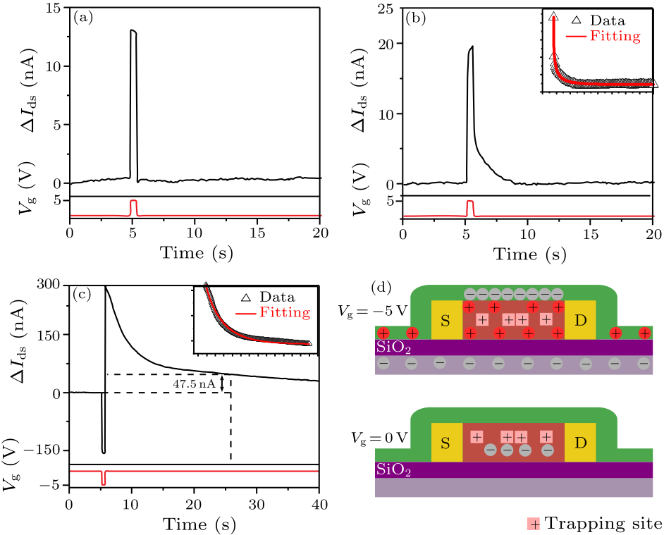
Fig. 3. Effects of short- and long-term memories of plasma-treated FETs. (a) Relative channel current ($\Delta I_{\rm ds}$) in response to a gate pulse, before plasma treatment, and (b) $\Delta I_{\rm ds}$ in response to a gate pulse after plasma treatment, showing short-term memory. Inset: stretched exponential decay fitting to the data in the main panel with a retention time of 0.18 s. (c) Long-term memory is achieved by applying a negative gate pulse to a plasma treated SnSe$_{2}$ FET. The dashed lines show that at 20 s after the pulse, $\Delta I_{\rm ds}\approx 47.5$ nA. Inset: stretched exponential decay fitting to the data in the main panel with a retention time of 4 s. (d) Model to explain the long-term memory. The channel contains hole trap sites represented by the squares with a $+$ sign, while circles with either $+$ or $-$ sign are mobile charge carriers (ions in the water film and holes or electrons in the channel).
In conclusion, we have found a new effect of plasma treatment. Due to the hydrophilicity change of the sample, a film of water automatically forms on the plasma treated device in the ambient moisture. The water film acts effectively as an ion liquid, hence the capacitive coupling between the back gate and the channel is enhanced by about two orders of magnitude. The ions and hole traps in these systems have slow dynamics, which have been used to realize a synaptic transistor with both the short-term and long-term memory effects. Our findings demonstrate the tremendous influence of plasma treatment on the electrical properties of 2D devices and provide insights for facile realization of neuromorphic devices. We thank Youdi Hu in ShanghaiTech University for the help with the water contact angle measurements. We thank Dr. Zhiqiang Zou and Dr. Xia Wang for the assistance with the PPMS measurements.
References Two-dimensional quasi-freestanding molecular crystals for high-performance organic field-effect transistorsImprovement of Performance of HfS 2 Transistors Using a Self-Assembled Monolayer as Gate DielectricSurface transfer doping induced effective modulation on ambipolar characteristics of few-layer black phosphorusStable few-layer MoS 2 rectifying diodes formed by plasma-assisted dopingSurface Functionalization of Black Phosphorus via Potassium toward High-Performance Complementary DevicesLayer-by-Layer Thinning of MoS 2 by PlasmaHigh-Performance 2D Rhenium Disulfide (ReS 2 ) Transistors and Photodetectors by Oxygen Plasma TreatmentPlasma-Treated Thickness-Controlled Two-Dimensional Black Phosphorus and Its Electronic Transport PropertiesArgon Plasma Induced Phase Transition in Monolayer MoS 2Producing air-stable monolayers of phosphorene and their defect engineeringFew-layer SnSe 2 transistors with high on/off ratiosField-effect transistors of high-mobility few-layer SnSe 2Air-Stable n-Doping of WSe 2 by Anion Vacancy Formation with Mild Plasma TreatmentTwo-dimensional lateral heterojunction through bandgap engineering of MoS 2 via oxygen plasmaTuning the electrical property via defect engineering of single layer MoS 2 by oxygen plasmaPhoton-induced selenium migration in TiSe 2High-Performance Flexible Graphene Field Effect Transistors with Ion Gel Gate DielectricsHighly Flexible MoS 2 Thin-Film Transistors with Ion Gel DielectricsImproved Carrier Mobility in Few-Layer MoS 2 Field-Effect Transistors with Ionic-Liquid GatingControlled Electrochemical Intercalation of Graphene/ h- BN van der Waals HeterostructuresModulation of the Electrical Properties of VO 2 Nanobeams Using an Ionic Liquid as a Gating MediumLow-voltage operation of a pentacene field-effect transistor with a polymer electrolyte gate dielectricThick Layered Semiconductor Devices with Water Top-Gates: High On–Off Ratio Field-Effect Transistors and Aqueous SensorsImmunocytochemical evidence for inhibitory and disinhibitory circuits in the superior oliveArtificial synapse network on inorganic proton conductor for neuromorphic systemsShort-Term Memory to Long-Term Memory Transition in a Nanoscale MemristorOrigin of Stretched Exponential Relaxation for Hopping-Transport ModelsSynaptic stability and plasticity in a floating world
[1] He D, Zhang Y, Wu Q et al 2014 Nat. Commun. 5 5162
[2] Zhang W L 2019 Chin. Phys. Lett. 36 067301
[3] Xiang D, Han C, Wu J et al 2015 Nat. Commun. 6 6485
[4] Chen M, Nam H, Wi S et al 2013 Appl. Phys. Lett. 103 142110
[5] Han C, Hu Z, Gomes L C et al 2017 Nano Lett. 17 4122
[6] Liu Y L, Nan H Y, Wu X et al 2013 ACS Nano 7 4202
[7] Shim J, Oh A, Kang D H et al 2016 Adv. Mater. 28 6985
[8] Jia J, Jang S K, Lai S et al 2015 ACS Nano 9 8729
[9] Zhu J Q, Wang Z C, Yu H et al 2017 J. Am. Chem. Soc. 139 10216
[10] Pei J J, Gai X, Yang J et al 2016 Nat. Commun. 7 10450
[11] Pei T, Bao L, Wang G et al 2016 Appl. Phys. Lett. 108 053506
[12] Guo C L, Tian Z, Xiao Y J et al 2016 Appl. Phys. Lett. 109 203104
[13] Tosun M, Chan L, Amani M et al 2016 ACS Nano 10 6853
[14] Choudhary N, Islam M R, Kang N et al 2016 J. Phys.: Condens. Matter 28 364002
[15] Islam M R, Kang N, Bhanu U et al 2014 Nanoscale 6 10033
[16] Lioi D B, Gosztola D J, Wiederrecht G P et al 2017 Appl. Phys. Lett. 110 081901
[17] Kim B J, Jang H, Lee S K et al 2010 Nano Lett. 10 3464
[18] Pu J, Yomogida Y, Liu K K et al 2012 Nano Lett. 12 4013
[19] Perera M M, Lin M W, Chuang H J et al 2013 ACS Nano 7 4449
[20] Zhao S Y F, Elbaz G A, Bediako D K et al 2018 Nano Lett. 18 460
[21] Ji H, Wei J and Natelson D 2012 Nano Lett. 12 2988
[22] Panzer M J, Newman C R and Frisbie C D 2005 Appl. Phys. Lett. 86 103503
[23] Huang Y, Sutter E, Wu L M et al 2018 ACS Appl. Mater. Interfaces 10 23198
[24] Smith A J, Owens S and Forsythe I D 2000 J. Physiol. 529 681
[25] Zhu L Q, Wan C J, Guo L Q et al 2014 Nat. Commun. 5 3158
[26] Chang T, Jo S H and Lu W 2011 ACS Nano 5 7669
[27] Sturman B, Podivilov E and Gorkunov M 2003 Phys. Rev. Lett. 91 176602
[28] Gerrow K and Triller A 2010 Curr. Opin. Neurobiol. 20 631