Chinese Physics Letters, 2022, Vol. 39, No. 4, Article code 045201 Atomically Dispersed Ni Single-Atoms Anchored on N-Doped Graphene Aerogels for Highly Efficient Electromagnetic Wave Absorption Bing Suo (索冰), Xiao Zhang (张潇)*, Xinyu Jiang (姜心雨), Feng Yan (闫峰)*, Zhengzhi Luo (罗正智), and Yujin Chen (陈玉金)* Affiliations Key Laboratory of In-Fiber Integrated Optics (Ministry of Education), and College of Physics and Optoelectronic Engineering, Harbin Engineering University, Harbin 150001, China Received 15 December 2021; accepted 9 March 2022; published online 28 March 2022 *Corresponding authors: Email: chenyujin@hrbeu.edu.cn; yanfeng@hrbeu.edu.cn; zhangxiaochn@hrbeu.edu.cn Citation Text: Suo B, Zhang X, Jiang X Y et al. 2022 Chin. Phys. Lett. 39 045201    Abstract Uniformly dispersed nickel single atoms (SAs) are experimentally prepared on ultralight N-doped graphene aerogels (Ni-SA@NRGA). The experimental results show that Ni-SAs in graphene aerogels can improve the conduction, polarization losses, and impedance matching properties of the Ni-SA@NRGA. As a result, the minimum reflection loss ($R_{\rm L,min}$) of Ni-SA@NRGA is $-$49.46 dB with a matching thickness of 2.0 mm and the broadest efficient absorption bandwidth is 3.12 GHz at a low thickness of 1.5 mm. Meanwhile, even with a matching thickness of 1.2–2.0 mm, the $R_{\rm L,min}$ value of Ni-SA@NRGA can reach $-$20 dB. The current study demonstrates the significance of incorporating metal single atoms into graphene aerogel for electromagnetic wave absorption.
cpl-39-4-045201-fig1.png
cpl-39-4-045201-fig2.png
cpl-39-4-045201-fig3.png
cpl-39-4-045201-fig4.png
cpl-39-4-045201-fig5.png
DOI:10.1088/0256-307X/39/4/045201 © 2022 Chinese Physics Society Article Text The rapid development of high-frequency electronic devices causes electromagnetic pollution and interference, endangering human health and the living environment. Meanwhile, electromagnetic waves (EMWs) interfere with the normal operation of sensitive electrical devices.[1,2] To eliminate electromagnetic pollution and interference, researchers have developed various EMW absorbing materials such as ferrite, ceramics, carbon-based materials, conductive polymers, and magnetic metal particles over the last several decades. These traditional absorbing materials have some drawbacks such as narrow effective absorption bandwidth (EAB) and thick matching thickness.[3] As a result, it is important to develop EMW absorbing materials with low density, thin matching thickness, intense absorption ability, and wide absorption bandwidth.[4–7] Graphene has become a research hotspot in EMW absorption (EWA) in recent years due to its superior specific surface area, low density, and high electrical conductivity.[8,9] However, if graphene is only used as an absorption material, it is difficult to tune its absorption bandwidth, impedance matching property, and absorption capacity.[9] Recently, it was found that fabrication of graphene aerogels (GAs) could significantly improve the EWA property of graphene-based absorbers. There were numerous hierarchical pores and three-dimensional (3D) networks in GAs, which not only gave a GA a high specific surface area and ultralow density but also effectively prevented the agglomeration of thin graphene sheets.[10] Furthermore, the multiple scattering of the EM wave in a GA makes it easier to improve the absorption property of the GA. Nevertheless, the absorption of pure GAs was not satisfactory due to lack of other loss factors. To increase dielectric loss factors, foreign magnetic nanomaterials such as Fe, Co, and Ni nanoparticles were introduced into GAs to increase the dielectric loss factors. For instance, Hu et al. synthesized 3D GA containing Fe$_{3}$O$_{4}$ nanocrystals, in which the synergistic effect between polarization and magnetic losses improved EWA performance.[11] Noticeably, the introduction of foreign materials increases the mass density and decreases the specific surface area of the GAs, affecting the lightweight property of the GA composites. Metal single atoms (M-SAs) have recently received a great deal of attention in electrocatalysis because of their ultra-high surface free energy, high atomic dispersion, and high atomic utilization efficiency.[12] M-SAs coordinated with nitrogen species (M-N$_{x}$) anchored on the carbon matrix, in particular, have good stability and have been widely investigated for catalyzing various chemical reactions.[13] Because of the different electronegativities of the metal, nitrogen, and carbon atoms, electrons around M-N$_{x}$ moieties would redistribute.[14] Electronic interactions between atoms and charge redistribution can change the electrical conductivity and create a local polarization system, which could promote the EWA property of the carbonaceous materials containing M-N$_{x}$ moieties. More importantly, unlike nanoparticles, the introduction of M-SAs into nanocarbons has no significant effect on mass density. As a result, M-SAs anchored nanocarbons have potential applications in lightweight EM absorbers. However, to the best of our knowledge, no high-performance GA containing uniform M-SAs has been reported so far. In this study, we propose a simple method for anchoring Ni-SAs on the N-doped GAs (Ni-SA@NRGA) for EWA. The as-prepared Ni-SA@NRGA exhibits good absorption performance with thickness in the range of 1.5–5.0 mm, an EAB of 3.12 GHz, and an $R_{\rm L,min}$ of $-$49.46 dB at 10.64 GHz. The increased dielectric loss as well as the unique 3D porous structure of Ni-SA@NRGA contributes to its high absorption performance. The NRGA, Ni-NP@NRGA, and Ni-SA@NRGA synthesis processes were thoroughly described in the Supplementary Material. The synthesis of Ni-SA@NRGA is depicted in Fig. 1. The graphene oxide was dispersed in distilled water using ultrasound, then hydrothermally treated at 180 ℃ for 10 h before being freeze-dried to form GAs. The mixture was then hydrothermally treated at 180 ℃ for 2 h with a piece of GAs, nickel chloride hexahydrate (NiCl$_{2}\cdot$6H$_{2}$O), and dicyandiamide (DCD) dispersed in 50 mL ethanol/water (volume : volume = $1\!:\!1$). The sample obtained in this stage was annealed at 900 ℃ for 2 h to produce GAs containing Ni nanoparticles (Ni-NPs), denoted as Ni-NP@NRGA. Finally, the Ni-NP@NRGA was immersed in a 2 M H$_{2}$SO$_{4}$ solution to remove the Ni nanoparticles, and Ni-SA@NRGA was obtained. The digital photographs of the as-fabricated NRGA, Ni-NP@NRGA, and Ni-SA@NRGA are shown in Fig. S1 in the Supplementary Material. The NRGA mass density was estimated to be around 0.0110 g/cm$^{3}$. The density increased to about 0.0187 g/cm$^{3}$ after the addition of the Ni-NPs, implying that the addition of the Ni-NPs suppresses the lightweight feature of the NRGA. The mass density of Ni-SA@NRGA, on the other hand, is reduced to 0.0141 g/cm$^{3}$, which is slightly higher than that of the pure NRGA. As a result, anchoring the Ni-SAs has little effect on the NRGA's lightweight feature. Ni contents in Ni-SA@NRGA and Ni-NP@NRGA are approximately 3.36 and 46.91 wt%, respectively, as determined by inductively coupled plasma-optical emission spectrometry (ICP-OES). Images from scanning electron microscopy (SEM) and transmission electron microscope (TEM) show that N-doped graphene (NG) has a curly sheet-like morphology [Figs. S3(a) and S3(b)]. Micropores can be seen in the graphene sheets, which aid in the anchoring of the M-SAs. The TEM images and element mappings show the coexistence of C, N, and O atoms in the NRGA [Fig. S3(d)], demonstrating N doping into graphene.[15] The surface oxygen-containing functional groups are responsible for the O signals. Ni-NP@NRGA SEM images [Fig. S4(a)] show that some large nanoparticles (50–300 nm) are distributed on the graphene sheet or wrapped by the graphene layer. The nanoparticles are metal Ni particles according to the TEM images and element mappings. Moreover, the Ni signals are also observed in the region without Ni nanoparticles, suggesting that the Ni-SAs are formed and anchored on the NG. Furthermore, the C, N, and O signals are observed, indicating that, in addition to Ni nanoparticles, surface oxygen-containing functional groups existed in the Ni-NP@NRGA.
cpl-39-4-045201-fig1.png
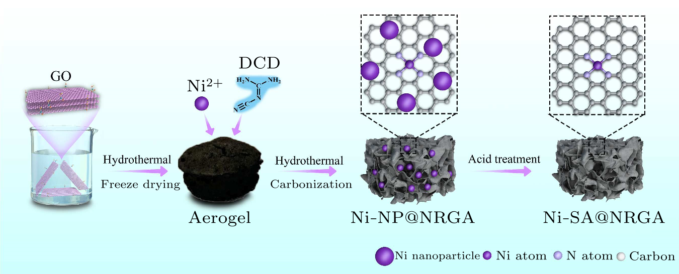
Fig. 1. Schematic illustration of the fabrication process of the Ni-SA@NRGA.
The Ni-SA@NRGA SEM image demonstrates that the NRGA's sheet-like morphology has been preserved [Fig. 2(a)]. The SEM image of Ni-SA@NRGA (Fig. S2) reveals that the aerogel is porous, with an average pore size of 13 µm. The inset of Fig. 2(a) shows that the Ni-SA@NRGA can be supported by Setaria Viridis, confirming its ultralight nature. The TEM images [Figs. 2(b) and 2(c)] show that metallic nanoparticles and clusters are missing from the Ni-SA@NRGA, indicating that the Ni nanoparticles were completely removed during the acid etching process. In addition, micropores can be found in the N-doped sheets. The aberration-corrected high-angle annular dark-field scanning transmission electron microscopy (AC-HAADF-STEM) image shows that some bright spots are evenly distributed on the NG, which correspond to the heavy Ni single atoms [Fig. 2(d)].[16]
cpl-39-4-045201-fig2.png
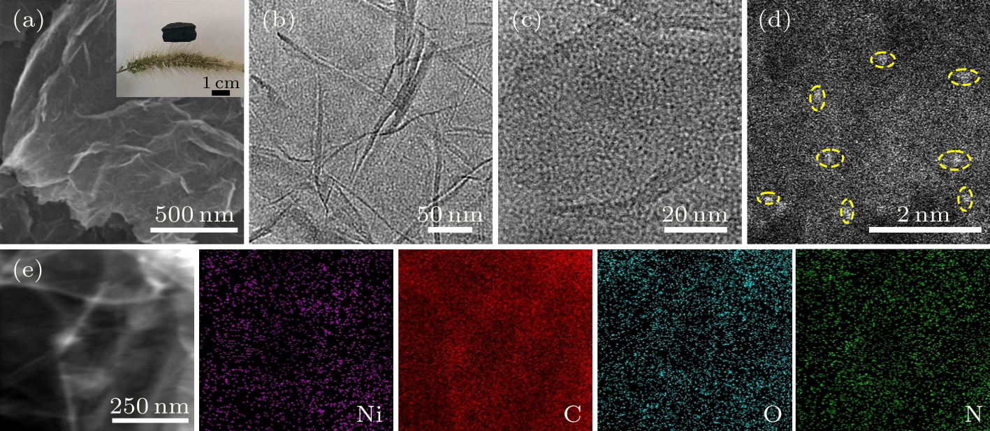
Fig. 2. (a) SEM image of the Ni-SA@NRGA, with the inset showing the digital photograph of Ni-SA@NRGA on the Setaria Viridis. (b) TEM image of the Ni-SA@NRGA. (c) HRTEM image of the Ni-SA@NRGA. (d) AC-HAADF-STEM image of the Ni-SA@NRGA. (e) TEM image and the corresponding EDX Ni, C, O, and N mappings of Ni-SA@NRGA.
cpl-39-4-045201-fig3.png
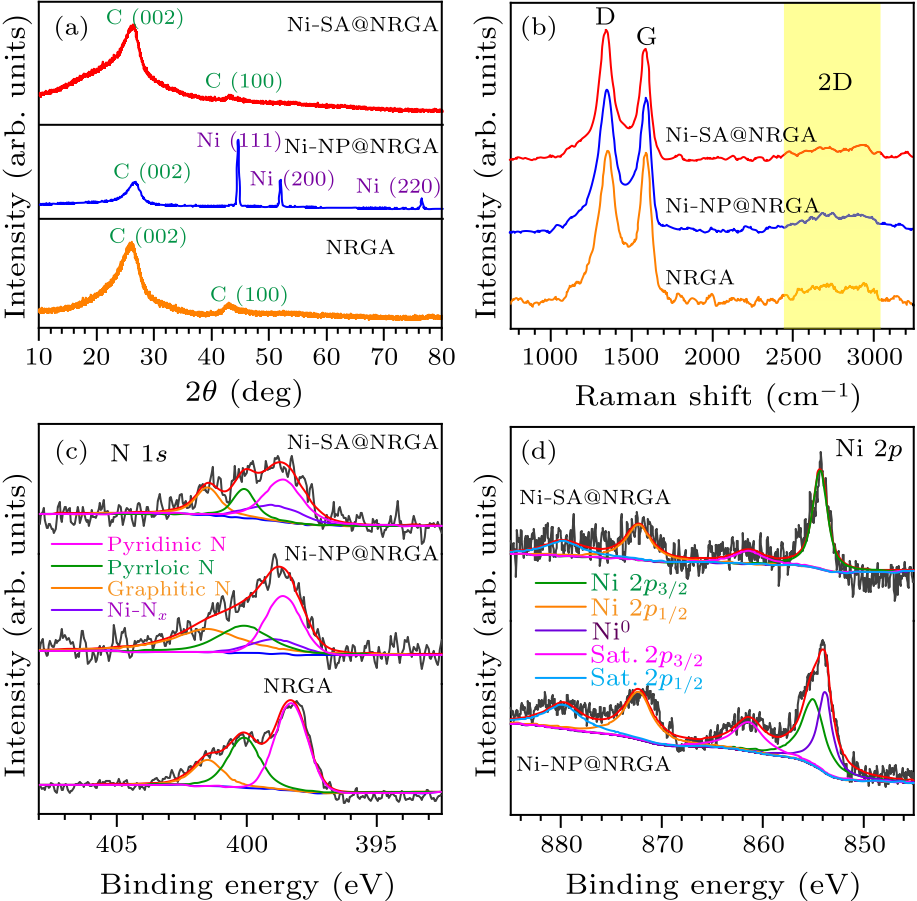
Fig. 3. (a) XRD patterns and (b) Raman spectra of Ni-SA@NRGA, Ni-NP@NRGA, and NRGA. (c) XPS spectra of N $1s$ of NRGA, Ni-SA@NRGA, and Ni-NP@NRGA. (d) XPS spectra of Ni $2p$ of Ni-SA@NRGA and Ni-NP@NRGA.
To further characterize the crystal structure and composition of the sample, Fig. 3(a) shows the x-ray diffraction (XRD) patterns of the samples. Two diffraction peaks at 26.3$^{\circ}$ and 43.0$^{\circ}$ in the NRGA and Ni-SA@NRGA XRD patterns correspond to the (002) and (100) planes of graphitic carbon (JCPDS card No. 41-1487), respectively.[17] The diffraction peaks of the Ni metals are not shown, revealing the absence of the Ni nanoparticles or clusters in two samples. The XRD pattern of Ni-NP@NRGA, on the other hand, shows diffraction peaks at 44.5$^{\circ}$, 51.8$^{\circ}$, and 76.3$^{\circ}$, which can be indexed to (111), (200), and (220) planes of cubic Ni (JCPDS card No. 04-0850), respectively.[18] Figure 3(b) shows the Raman spectra of Ni-SA@NRGA, Ni-NP@NRGA, and NRGA. In the Raman spectra, the two peaks of carbon-based materials at 1351 and 1591 cm$^{-1}$ correspond to the D-band and G-band, respectively.[19] The intensity ratios ($I_{\rm D}/I_{\rm G}$) of Ni-SA@NRGA, Ni-NP@NRGA, and NRGA are 1.17, 1.06, and 1.03, respectively, indicating that Ni-SA@NRGA has the least degree of graphitization with abundant edge defects. Furthermore, 2D peaks of aerogels can be found in Raman spectra, indicating graphene multilayer properties.[20] x-ray photoelectron spectroscopy (XPS) shows the presence of Ni, C, N, and O elements in Ni-SA@NRGA and Ni-NP@NRGA, while C, N, and O elements in NRGA (Fig. S6). Three typical characteristic peaks of high-resolution C $1s$ XPS spectra of Ni-SA@NRGA, Ni-NP@NRGA, and NRGA located at 284.6, 285.1, and 286.2 eV correspond to the C–C, C–N, and C–O/C=O groups in Fig. S5, respectively.[4] The N $1s$ XPS spectra of Ni-SA@NRGA and Ni-NP@NRGA are shown in Fig. 3(c), with binding energies centered at 401.5, 398.9, 400.1, and 398.6 eV, which could correspond to graphitic-N, Ni-N$_{x}$, pyrrolic-N, and pyridinic-N, respectively.[4,21] In contrast, the Ni-N$_{x}$ species are not detected in the NRGA XPS spectra, implying that no Ni-SAs are present in the sample (Fig. S6). The high-resolution Ni $2p$ XPS spectrum of Ni-SA@NRGA, as shown in Fig. 3(d), shows two peaks at about 854.3 eV (Ni $2p_{3/2}$) and 872.3 eV (Ni $2p_{1/2}$), which can be attributed to the Ni-N$_{x}$ species, with satellite peaks at 861.4 and 879.8 eV.[21,22] There are no metallic nickel signals observed, indicating that the Ni species are primarily anchored on the NG in the form of SAs. In contrast, metallic Ni with a binding energy of 853.8 eV was detected in the Ni $2p$ XPS spectra of Ni-NP@NRGA, in addition to the Ni-N$_{x}$ species [Fig. 3(d)].[23] The binding energies of the Ni-N$_{x}$ in the Ni-NP@NRGA shift negatively when compared to the Ni-SA@NRGA, indicating an electronic interaction between metallic Ni nanoparticles and Ni-N$_{x}$. A sample vibration magnetometer was used to measure the magnetic properties of the Ni-SA@NRGA and Ni-NP@NRGA. The magnetization hysteresis loops show that Ni-NP@NRGA with Ni particles is ferromagnetic, whereas Ni-SA@NRGA with Ni single atoms is diamagnetism, confirming the complete removal of Ni-NPs in the Ni-SA@NRGA sample (Fig. S7).[24,25] The EM parameters of samples with a filler ratio of 25 wt% in the paraffin matrix were determined. The reflection loss ($R_{\rm L}$) and the effective absorbance (EAB) are important criteria for evaluating the absorbing performance of the samples. Based on the transmission line theory, the $R_{\rm L}$ was calculated based on the measured electromagnetic parameters [Eqs. (S1) and (S2) in Supporting Information].[26–28] The NRGA's $R_{\rm L,min}$ was only $-$30.12 dB at a thickness of $d=5.0$ mm, and its EAB is only 2.0 GHz with $d=2.5$ mm, indicating poor absorption performance [Fig. S8(a)]. The absorption property was improved significantly after the addition of Ni nanoparticles. The minimum $R_{\rm L}$ value of Ni-NP@NRGA is $-$40.53 dB at 4.72 GHz with $d=4.5$ mm, and the largest EAB is increased to 2.24 GHz with $d = 2.5$ mm, as shown in Fig. 4(a). If the Ni nanoparticles were removed, the absorption property was further improved. As illustrated in Fig. 4(b), the $R_{\rm L,min}$ value of Ni-SA@NRGA is $-$49.46 dB with $d = 2.0$ mm, and its largest EAB is 3.12 GHz with a small $d = 1.5$ mm. Furthermore, when $d$ is within the scope of 1.5–5.0 mm, the $R_{\rm L,min}$ values of Ni-SA@NRGA exceed $-$10 dB. Furthermore, even if the matching thickness is in the range of 1.2–2.0 mm, the $R_{\rm L,min}$ value of Ni-SA@NRGA can exceed above $-$20 dB [Fig. 4(c)]. As a result, Ni-SA@NRGA has better EMW absorption performance than that of the NRGA and the Ni-NP@NRGA, demonstrating that the incorporation of Ni-SAs into the NRGA is beneficial to improving the EWA performance. Furthermore, in terms of thickness or filler ratio, the absorption property of the Ni-SA@NRGA is comparable or superior to the magnetic carbon-based absorbers, implying that it has promising applications in the EWA field (Table S1).[29–32]
cpl-39-4-045201-fig4.png
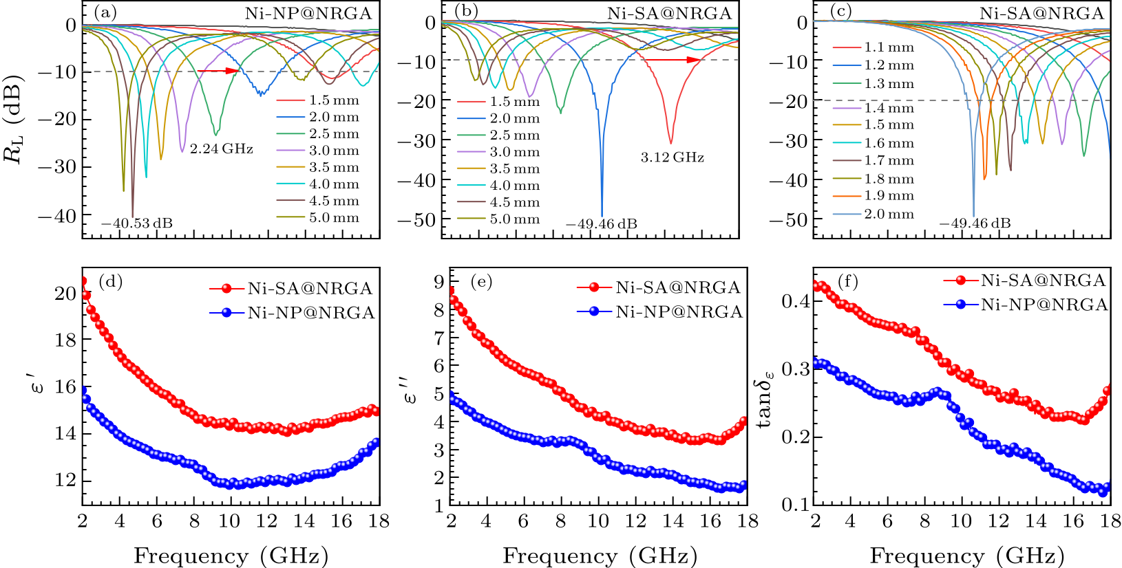
Fig. 4. (a) $R_{\rm L}$–$f$ curves of Ni-NP@NRGA with thickness of 1.5–5.0 mm. (b) $R_{\rm L}$–$f$ curves of Ni-SA@NRGA with thickness of 1.5–5.0 mm. (c) $R_{\rm L}$–$f$ curves of Ni-SA@NRGA with thickness of 1.1–2.0 mm. (d)–(f) Behaviors of $\varepsilon'$, $\varepsilon ''$ and tan$\delta_{\varepsilon}$ of the complex permittivity and loss tangents of the Ni-SA@NRGA and Ni-NP@NRGA samples.
The electromagnetic parameters of Ni-SA@NRGA and Ni-NP@NRGA are compared for determining the reasons of the enhanced electromagnetic absorption performance of Ni-SA@NRGA. The real parts ($\varepsilon'$) of the complex permittivity of Ni-SA@NRGA and Ni-NP@NRGA as a function of frequency are shown in Fig. 4(d). The $\varepsilon '$ values of the samples gradually decrease with increasing frequency in the low-frequency region ($\lesssim $ 10 GHz), and then slightly rise in the high-frequency region, which may be due to the enhancement of the polarization relaxations in the high-frequency region.[33] Over 2–18 GHz, the $\varepsilon '$ values of Ni-SA@NRGA (14.07– 20.41) are significantly higher than those of Ni-NP@NRGA (11.81–15.83). Simultaneously, as shown in Fig. 4(e), the imaginary parts ($\varepsilon ''$) of the complex permittivity of Ni-SA@NRGA are changed in the range of 3.28–8.67, which is larger than that of Ni-NP@NRGA (1.59–4.93). The larger $\varepsilon '$ and $\varepsilon ''$ values of the Ni-SA@NRGA imply that it has better EMW energy and attenuation abilities. Furthermore, the dielectric loss tangent (tan$\delta_{\varepsilon} =\varepsilon ''/\varepsilon '$) of the Ni-SA@NRGA varies in the range of 0.22–0.42, which is greater than that of the Ni-NP@NRGA (0.11–0.35), indicating that the Ni-SA@NRGA has improved dielectric loss performance over the Ni-NP@NRGA [Fig. 4(f)]. As a result, the improved absorption property of Ni-SA@NRGA can be attributed to its increased dielectric loss. Furthermore, the $\varepsilon '$ and $\varepsilon ''$ values of the NRGA are lower than those of Ni-SA@NRGA [Figs. S8(b) and S8(c)]. As a result, the NRGA has lower tan$\delta_{\varepsilon}$ values [Fig. S9(c)], leading to its inferior EWA property to that of Ni-SA@NRGA.
cpl-39-4-045201-fig5.png
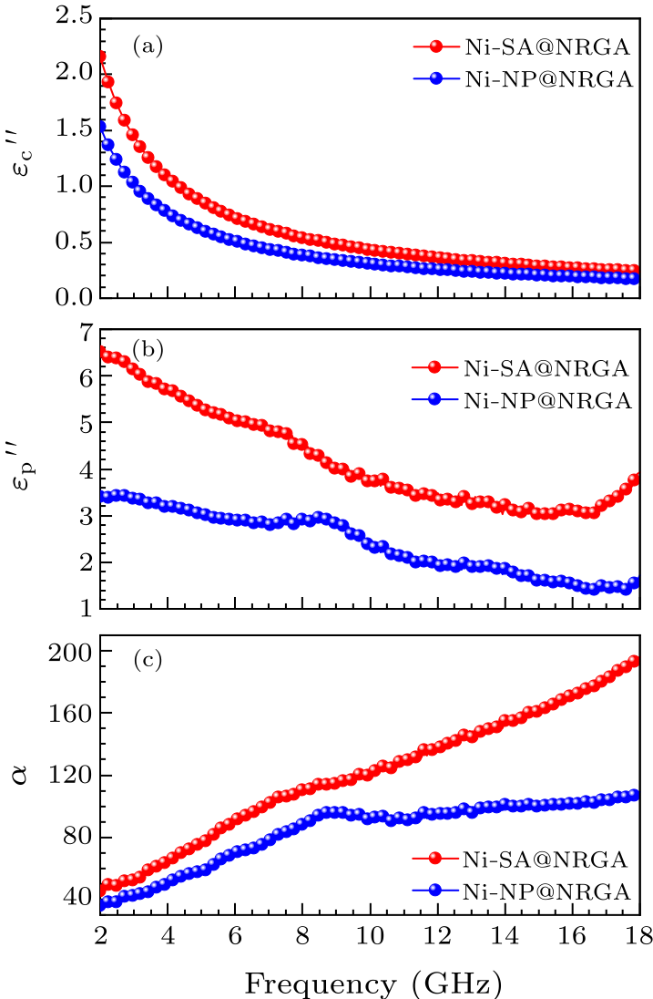
Fig. 5. (a) Conductive loss and (b) polarization loss of Ni-SA@NRGA and Ni-NP@NRGA. (c) The attenuation coefficients of Ni-SA@NRGA and Ni-NP@NRGA.
To understand the difference in dielectric loss between the samples, the sources of $\varepsilon ''$ of the samples were analyzed. In general, $\varepsilon ''$ of a dielectric material includes conduction loss ($\varepsilon_{\rm c}''$) and polarization relaxation loss ($\varepsilon_{\rm p}''$).[21] The straight line and the semicircle in the Cole–Cole plots indicate that the three samples have both conduction and polarization relaxation losses (Fig. S11).[34] The measured $\sigma$ values by an electrochemical station in a low-frequency range were 0.24, 0.17, and 0.14 S m$^{-1}$ for Ni-SA@NRGA, Ni-NP@NRGA, and NRGA, respectively. According to the values, $\varepsilon_{\rm c}''$ values of the samples were estimated. The conductivity losses of Ni-SA@NRGA are higher than those of Ni-NP@NRGA and NRGA, as shown in Figs. 5(a) and S9(a), especially at low frequencies. Meanwhile, the $\varepsilon_{\rm p}''$ values of Ni-SA@NRGA are also much higher than those of Ni-NP@NRGA and NRGA [Figs. 5(b) and S9(b)]. As previously reported, the introduction of M-SAs into a nanocarbon matrix regulates the electronic structure of the adjacent carbon atoms, increasing the electrical conductivity of the nanocarbon containing M-SAs.[14] As a result, the increased conduction loss of the Ni-SA@NRGA is understandable. Meanwhile, polarization systems would be created by combining M-SAs with nanocarbons, causing charge transfer due to the different electronegativities of the metal, nitrogen, and carbon atoms. The interaction of the M-SAs-containing nanocarbons with EMW could induce polarization loss in the formed polarization systems, increasing the polarization loss.[14,35] As a result, the improved dielectric loss performance of the Ni-SA@NRGA is attributed to increases in both $\varepsilon_{\rm c}''$ and $\varepsilon_{\rm p}''$, which are greater than those of Ni-NP@NRGA and NRGA. Figure S10 shows the comparison of relatively complex permeability for the three samples. It is found that the tan$\delta_{\mu} =\mu''/\mu'$ values ($\mu'$ and $\mu''$ are real and imaginary parts of the complex permeability, respectively) are less than 0.13, indicating that magnetic loss is not a significant factor in the EWA properties of the three samples. Aside from dielectric and magnetic losses, absorbers impedance matching characteristic is also an important factor in its EWA property. To assess the degree of impedance matching, one can use the impedance characteristic $|Z| =|Z_{\rm in}/Z_{0}|$ [Eq. (S3)]. If $|Z|$ is infinitely close to 1, the absorber has the best impedance matching characteristic, making it easier to improve EWA.[36] The $|Z| $–$f$ plots of Ni-SA@NRGA, Ni-NP@NRGA, and NRGA are shown in Figs. S12(a)–S12(c). When $d$ is in the range 1.5–2.0 mm, the $|Z|$ values of Ni-SA@NRGA are closer to 1 compared to Ni-NP@NRGA and NRGA. Thus, the improved EWA property of the Ni-SA@NRGA is related to its improved impedance matching performance. In addition to the EWA property, an absorber's attenuation ability is critical for its practical application. The attenuation coefficient $\alpha$ can be used to evaluate an absorber's attenuation ability [Eq. (S4)].[37] As shown in Fig. 5(c), the $\alpha$ values of Ni-SA@NRGA vary in the range 49.8–181.1 over 2–18 GHz, which is higher than the values of Ni-NP@NRGA (35.9–109.1) and NRGA (33.3–115.2), indicating that Ni-SA@NRGA has better attenuation ability toward the EMW. The strong EWA property and attenuation ability of Ni-SA@NRGA are a potential candidate for the EWA field.[38,39] In summary, we have used a simple method to create ultralight NG aerogels with anchoring uniform dispersion of nickel single atoms (Ni-SA@NRGA). As lightweight EMW absorbers, the Ni-SA@NRGA exhibits outstanding EWA performance with a minimum $R_{\rm L}$ of $-$49.46 dB and a thickness of only 2.0 mm, and its largest EAB is up to 3.12 GHz (below $-$10 dB). The results indicate that introduction of Ni-SAs and coordinated with nitrogen species (M-N$_{x}$) immobilized on carbon matrix can raise dielectric loss aroused by conductive loss, polarization relaxation. Furthermore, the multiple scattering of the Ni-SA@NRGA porous structure improves EWA performance, outperforming most reported carbon-based EMW absorbing materials. As a result, it is thought that this work provides new ideas and methods for a new pattern of EWA materials with higher $R_{\rm L}$, a wider absorption frequency boundary, and lighter weight. Acknowledgements. This work was supported by the National Natural Science Foundation of China (Grant No. 51972077), the Heilongjiang Touyan Innovation Team Program, and the Fundamental Research Funds for the Central Universities (Grant Nos. 3072020CF2518, 3072020CFT2505, and 3072020CFJ2503).
References Biomass-derived graphene-like porous carbon nanosheets towards ultralight microwave absorption and excellent thermal infrared propertiesNitrogen and Boron Co-Doped Carbon Nanotubes Embedded with Nickel Nanoparticles as Highly Efficient Electromagnetic Wave Absorbing MaterialsUltralight, highly compressible and fire-retardant graphene aerogel with self-adjustable electromagnetic wave absorptionLarge-Scale Synthesis of Three-Dimensional Reduced Graphene Oxide/Nitrogen-Doped Carbon Nanotube Heteronanostructures as Highly Efficient Electromagnetic Wave Absorbing MaterialsMicrowave Absorption Enhancement and Complex Permittivity and Permeability of Fe Encapsulated within Carbon NanotubesCross-Stacking Aligned Carbon-Nanotube Films to Tune Microwave Absorption Frequencies and Increase Absorption IntensitiesCoNi@SiO2 @TiO2 and CoNi@Air@TiO2 Microspheres with Strong Wideband Microwave AbsorptionHollow N-Doped Carbon Polyhedron Containing CoNi Alloy Nanoparticles Embedded within Few-Layer N-Doped Graphene as High-Performance Electromagnetic Wave Absorbing MaterialAdvances of 3D graphene and its composites in the field of microwave absorptionA review of three-dimensional graphene-based aerogels: Synthesis, structure and application for microwave absorption3D graphene–Fe3O4 nanocomposites with high-performance microwave absorptionGraphene-supported metal single-atom catalysts: a concise reviewSingle Nickel Atoms on Nitrogen‐Doped Graphene Enabling Enhanced Kinetics of Lithium–Sulfur BatteriesIdentification of the Intrinsic Dielectric Properties of Metal Single Atoms for Electromagnetic Wave AbsorptionSynthesis of three-dimensional porous netlike nitrogen-doped reduced graphene oxide/cerium oxide composite aerogels towards high-efficiency microwave absorptionUnsaturated edge-anchored Ni single atoms on porous microwave exfoliated graphene oxide for electrochemical CO2Ultralight CoNi/rGO aerogels toward excellent microwave absorption at ultrathin thicknessTailing size and impedance matching characteristic of nitrogen-doped carbon nanotubes for electromagnetic wave absorptionDesign of cellular structure of graphene aerogels for electromagnetic wave absorptionSynthesis, characterization and electromagnetic wave absorption properties of asphalt carbon coated graphene/magnetic NiFe2O4 modified multi-wall carbon nanotube compositesN-doped reduced graphene oxide aerogels containing pod-like N-doped carbon nanotubes and FeNi nanoparticles for electromagnetic wave absorptionSemi-sacrificial template synthesis of single-atom Ni sites supported on hollow carbon nanospheres for efficient and stable electrochemical CO2 reductionCoNi nanoparticles encapsulated by nitrogen-doped carbon nanotube arrays on reduced graphene oxide sheets for electromagnetic wave absorptionEnhanced (X-band) microwave shielding properties of pure magnesium by addition of diamagnetic titanium micro-particulatesSynthesis of magnetic graphene aerogels for microwave absorption by in-situ pyrolysisMicrowave Absorption Enhancement of Multifunctional Composite Microspheres with Spinel Fe3O4 Cores and Anatase TiO2 ShellsFabrication and microwave absorption of carbon nanotubes∕CoFe2O4 spinel nanocompositeEnhanced Microwave Absorption Performance from Magnetic Coupling of Magnetic Nanoparticles Suspended within Hierarchically Tubular CompositePreparation of graphene/Fe3 O4 /Ni electromagnetic microwave absorbing nano-composite materialsHexagonal and cubic Ni nanocrystals grown on graphene: phase-controlled synthesis, characterization and their enhanced microwave absorption propertiesFeNi3 alloy nanocrystals grown on graphene: Controllable synthesis, in-depth characterization and enhanced electromagnetic performanceOne-step hydrothermal synthesis and enhanced microwave absorption properties of Ni0.5Co0.5Fe2O4/graphene composites in low frequency bandTunable Dielectric Properties of Carbon Nanotube@Polypyrrole Core-Shell Hybrids by the Shell Thickness for Electromagnetic Wave Absorption*Three-dimensional nitrogen-doped reduced graphene oxide aerogel decorated with Ni nanoparticles with tunable and unique microwave absorptionAtomically dispersed cobalt anchored on N-doped graphene aerogels for efficient electromagnetic wave absorption with an ultralow filler ratioConstruction of C-Si heterojunction interface in SiC whisker/reduced graphene oxide aerogels for improving microwave absorptionUltralight graphene aerogel enhanced with transformed micro-structure led by polypyrrole nano-rods and its improved microwave absorption propertiesHydrophobic SiC@C Nanowire Foam with Broad-Band and Mechanically Controlled Electromagnetic Wave AbsorptionAlternating Multilayered Si3 N4 /SiC Aerogels for Broadband and High-Temperature Electromagnetic Wave Absorption up to 1000 °C
[1] Zhao H Q, Cheng Y, Zhang Z, Zhang B S, Pei C C, Fan F Y, and Ji G B 2021 Carbon 173 501
[2] Zhu X, Yan F, Li C Y, Qi L H, Yuan H R, Liu Y F, Zhu C L, and Chen Y J 2021 Chin. Phys. Lett. 38 015201
[3] Wang Z C, Wei R B, Gu J W, Liu H, Liu C T, Luo C J, Kong J, Shao Q, Wang N, Guo Z H, and Liu X B 2018 Carbon 139 1126
[4] Zhang X C, Xu J, Yuan H R, Zhang S, Ouyang Q Y, Zhu C L, Zhang X T, and Chen Y J 2019 ACS Appl. Mater. & Interfaces 11 39100
[5] Che R C, Peng L M, Duan X F, Chen Q, and Liang X L 2004 Adv. Mater. 16 401
[6] Sun H, Che R C, You X, Jiang Y S, Yang Z B, Deng J, Qiu L B, and Peng H S 2014 Adv. Mater. 26 8120
[7] Liu Q H, Cao Q, Bi H, Liang C Y, Yuan K P, She W, Yang Y J, and Che R C 2016 Adv. Mater. 28 486
[8] Zhang X, Yan F, Zhang S, Yuan H R, Zhu C L, Zhang X T, and Chen Y J 2018 ACS Appl. Mater. & Interfaces 10 24920
[9] Sultanov F, Daulbayev C, Bakbolat B, and Daulbayev O 2020 Adv. Colloid Interface Sci. 285 102281
[10] Zhi D D, Li T, Li J Z, Ren H S, and Meng F B 2021 Compos. Part B 211 108642
[11] Hu C G, Mou Z Y, Lu G W, Chen N, Dong Z L, Hu M J, and Qu L T 2013 Phys. Chem. Chem. Phys. 15 13038
[12] Ren S, Yu Q, Yu X H, Rong P, Jiang L Y, and Jiang J C 2020 Sci. Chin. Mater. 63 903
[13] Zhang L L, Liu D B, Muhammad Z, Wan F, Xie W, Wang Y J, Song L, Niu Z Q, and Chen J 2019 Adv. Mater. 31 1903955
[14] Zhang X C, Shi Y N, Xu J, Ouyang Q Y, Zhang X, Zhu C L, Zhang X L, and Chen Y J 2022 Nano-Micro Lett. 14 27
[15] Wu L Z, Shu R W, Zhang J B, and Chen X T 2022 J. Colloid Interface Sci. 608 1212
[16] Cheng Y, Zhao S Y, Li H B, He S, Veder J P, Johannessen B, Xiao J P, Lu S F, Pan J, Chisholm M F, Yang S Z, Liu C, Chen J G, and Jiang S P 2019 Appl. Catal. B: Environ. 243 294
[17] Zhao H B, Cheng J B, Zhu J Y, and Wang Y Z 2019 J. Mater. Chem. C 7 441
[18] Cao F H, Yan F, Xu J, Zhu C L, Qi L H, Li C Y, and Chen Y J 2021 Carbon 174 79
[19] Huang X G, Yu G Y, Zhang Y K, Zhang M J, and Shao G F 2021 Chem. Eng. J. 426 131894
[20] Zhang K C, Gao X B, Zhang Q, Li T P, Chen H, and Chen X F 2017 J. Alloys Compd. 721 268
[21] Xu J, Zhang X, Zhao Z B, Yuan H R, Zhang S, Zhu C L, Zhang X T, and Chen Y J 2020 Carbon 159 357
[22] Yuan C Z, Zhan L Y, Liu S J, Chen F, Lin H J, Wu X L, and Chen J R 2020 Inorg. Chem. Front. 7 1719
[23] Zhang X C, Zhang X, Yuan H R, Li K Y, Ouyang Q Y, Zhu C L, Zhang S, and Chen Y J 2020 Chem. Eng. J. 383 123208
[24] Pandey R, Tekumalla S, and Gupta M 2019 J. Alloys Compd. 770 473
[25] Xu D W, Yang S, Chen P, Yu Q, Xiong X H, and Wang J 2019 Carbon 146 301
[26] Liu J W, Che R C, Chen H J, Zhang F, Xia F, Wu Q S, and Wang M 2012 Small 8 1214
[27] Che R C, Zhi C Y, Liang C Y, and Zhou X G 2006 Appl. Phys. Lett. 88 033105
[28] Wu Z C, Pei K, Xing L S, Yu X F, You W B, and Che R C 2019 Adv. Funct. Mater. 29 1901448
[29] Huang Y W, Wang Y J, Wei S C, Liang Y, Huang W, Wang B, and Xu B S 2019 Int. J. Mod. Phys. B 33 1940055
[30] Chen T T, Deng F, Zhu J, Chen C F, Sun G B, Ma S L, and Yang X J 2012 J. Mater. Chem. 22 15190
[31] Ma T, Yuan M W, Islam S M, Li H F, Ma S L, Sun G B, and Yang X J 2016 J. Alloys Compd. 678 468
[32] Yin P F, Deng Y, Zhang L M, Wu W J, Wang J, Feng X, Sun X Y, Li H Y, and Tao Y 2018 Ceram. Int. 44 20896
[33] Wang D T, Wang X C, Zhang X, Yuan H R, and Chen Y J 2020 Chin. Phys. Lett. 37 045201
[34] Tang J M, Liang N, Wang L, Li J, Tian G, Zhang D, Feng S H, and Yue H J 2019 Carbon 152 575
[35] Xu J, Liu M J, Zhang X C, Li B, Zhang X, Zhang X L, Zhu C L, and Chen Y J 2022 Appl. Phys. Rev. 9 011402
[36] Chen J P, Jia H, Liu Z, Kong Q Q, Hou Z H, Xie L J, Sun G H, Zhang S C, and Chen C M 2020 Carbon 164 59
[37] Liu B, Li J H, Wang L F, Ren J H, and Xu Y F 2017 Compos. Part A 97 141
[38] Cai Z X, Su L, Wang H J, Niu M, Gao H F, Lu D, and Li M Z 2020 ACS Appl. Mater. & Interfaces 12 8555
[39] Cai Z X, Su L, Wang H J, Niu M, Tao L T, Lu D, Xu L, Li M Z, and Gao H F 2021 ACS Appl. Mater. & Interfaces 13 16704