Chinese Physics Letters, 2020, Vol. 37, No. 6, Article code 066802 Symmetry Breaking and Reversible Hydrogenation of Two-Dimensional Semiconductor Sn$_{2}$Bi * Xuguang Wang (王旭光)1,2, Bingyu Xia (夏炳煜)3, Jian Gou (苟建)1,2, Peng Cheng (程鹏)1,2, Yong Xu (徐勇)3, Lan Chen (陈岚)1,2**, Kehui Wu (吴克辉)1,2,4** Affiliations 1Institute of Physics, Chinese Academy of Sciences, Beijing 100190, China 2School of Physics, University of Chinese Academy of Sciences, Beijing 100049, China 3Department of Physics, Tsinghua University, Beijing 100084, China 4Collaborative Innovation Center of Quantum Matter, Beijing 100871, China Received 23 April 2020, online 26 May 2020 *Supported by the National Key Research and Development Program of China (Grant Nos. 2018YFE0202700, 2016YFA0202301, and 2016YFA0300904), the National Natural Science Foundation of China (Grant Nos. 11761141013, 11674366, 11825405, and 11674368), the Beijing Municipal Natural Science Foundation (Grant No. Z180007), and the Strategic Priority Research Program of the Chinese Academy of Sciences (Grant No. XDB30103000).
**Corresponding author. Email: lchen@iphy.ac.cn; khwu@iphy.ac.cn
Citation Text: Wang X G, Xia B Y, Gou J, Cheng P and Xu Y et al 2020 Chin. Phys. Lett. 37 066802    Abstract The hydrogenation of two-dimensional (2D) systems can efficiently modify the physical and chemical properties of materials. Here we report a systematic study on the hydrogenation of 2D semiconductor Sn$_{2}$Bi on Si(111) by scanning tunneling microscopy experiments and first principle calculations. The unique butterfly-like and trench-like features were observed for single H adsorption sites and hydrogen-saturated surfaces respectively, from which the bridge-site adsorption geometry can be unambiguously determined. The structural model was further confirmed by the theoretical calculations, which is in good agreement with the experimental observation. In addition, the hydrogenation is found to vanish the flat band of Sn$_{2}$Bi and increase the band gap obviously. DOI:10.1088/0256-307X/37/6/066802 PACS:68.35.bg, 68.37.Ef © 2020 Chinese Physics Society Article Text The hydrogenation of semiconductor surfaces is an important issue in surface science. Unlike metal surfaces, the interactions between the semiconductor surface and hydrogen atoms are weak but complex though hydrogen is the simplest atom. Hydrogen not only binds to the dangling bonds of the semiconductor surface, but also interacts with the underlying atomic layers below the surface.[1–7] Moreover, hydrogenation may change the electronic states[8–11] as well as the chemical reactivity of the semiconductor surface,[12] which is important for many applications. Two-dimensional (2D) materials have attracted considerable attention since the advent of graphene. Among them, 2D materials with honeycomb structures are particularly striking due to their particular quantum properties.[13–17] Recently, we synthesized new 2D monolayer semiconductors Sn$_{2}$Bi on Si(111) substrates, which have a unique double-honeycomb structure[18] and the specific electronic structure of Sn$_{2}$Bi, including the coexistence of a flat band in the conduction band and a nearly free hole band in the valence band. However, since scanning tunneling microscopy (STM) is unable to identify the chemical information of atoms, the structure model of Sn$_{2}$Bi–$2\times 2$ is so far mainly determined by theoretical calculations. Additional experimental evidence on the structure model is thus highly desirable. Furthermore, subsequent computational works reported that hydrogenation of Sn$_{2}$Bi nanosheets will stabilize and tailor its electronic and optical properties.[19–21] Therefore, it is necessary to experimentally investigate the hydrogenation of the Sn$_{2}$Bi system. In this study, we perform hydrogenation of the 2D Sn$_{2}$Bi. The original ideal situation was that hydrogen atoms may selectively adsorb on Sn or B atoms on the surface, which provides chemical information of the surface atoms. Indeed, we found unique butterfly-like features on the single H adsorption sites, from which one can unambiguously determine the adsorption geometry by simple symmetry analysis. Moreover, the adsorption of H atoms kills the flat band and expands the bandgap of the surface, which is consistent with the origination of the flat band from the central Sn atoms. Our results not only provide experimental support to the double-honeycomb lattice structure of 2D Sn$_{2}$Bi, but also demonstrate the interesting role of hydrogenation in the surface structural determination as well as the modification of surface electronic structures. The experiments were carried out in a home-built low-temperature scanning tunneling microscope (STM) system combined with a molecular beam epitaxy (MBE) chamber for sample preparation, where the base pressure was $1\times {10}^{-10}$ mbar. A clean Si(111) surface was obtained by the standard flashing procedure. High-purity Bi (99.999%) and Sn (99.999%) were evaporated from effusion cells. The Sn$_{2}$Bi layer was grown by a two-step process: first, slightly more than 1 monolayer (ML) of Bi were grown on the Si(111) surface held at room temperature,[22] followed by annealing the surface at 670 K for several minutes to obtain a surface with a single phase $\beta$-Si(111)-$\sqrt{3}\times\sqrt{3}$-Bi structure (1 ML is defined as the atomic density of the Si(111) plane). Then Sn atoms were deposited on the $\beta$-Si(111)-$\sqrt{3}\times\sqrt{3}$-Bi surface held at 470 K. This results in a nearly perfect surface with a single Sn$_{2}$Bi layer on top.[18] To adsorb hydrogen atoms on Sn$_{2}$Bi, high-purity hydrogen was introduced into the UHV chamber and cracked by a hot tungsten filament heated to about 2000 K to produce atomic hydrogen atoms. The partial and saturated hydrogen doses were 8 Langmuir and 90 Langmuir respectively (the partial pressure of hydrogen and exposure time were $3\times 10^{-8}$ mbar, 5 min and $2\times 10^{-7}$ mbar, 10 min, respectively). All the STM measurements were performed at 77 K, and the bias voltage was applied to the STM tip. First principles calculations were performed using the Vienna Ab Initio Simulation Package (VASP) toolkit. The model of the Si(111) substrate includes three Si bilayers, with the top bilayer relaxed during structural optimization and the bottom Si atoms saturated by hydrogen. Structural optimization was performed by applying a force convergence criterion of $001$ eV/Å and a Gaussian smearing of 0.05 eV together with a $5\times 5\times 1$ Monkhorst–Pack $k$ grid for $2 \times 2$ superstructures on Si(111).
cpl-37-6-066802-fig1.png
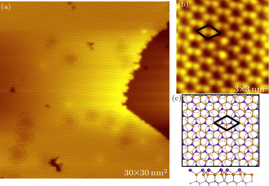
Fig. 1. STM image and structural model of clean Sn$_{2}$Bi on Si(111). (a) A typical topography image of a clean Sn$_{2}$Bi $2 \times 2$ surface (tip bias 2 V, tunneling current 100 pA). (b) Zoom-in image of the surface of (a) (tip bias $-1$ V, tunneling current 90 pA). The black rhombuses represent one unit cell. (c) Top and side views of the structural model of Sn$_{2}$Bi. Each unit cell consists of four Sn atoms and two upper-bulked Bi atoms. The gray balls are silicon atoms. The Sn atoms and Bi atoms are represented by yellow and purple balls, respectively.
Figures 1(a) and 1(b) show a typical large-area STM image and a high-resolution STM image of the as-prepared Sn$_{2}$Bi $2 \times 2$ surface respectively, exhibiting a single phase with characteristic honeycomb lattice covering the entire Si(111) substrate. The atomic structure of the Sn$_{2}$Bi $2 \times 2$ surface has been understood by a bulked double-honeycomb model as depicted in Fig. 1(c), in which the yellow balls represent lower-bulked Sn atoms and the purple balls are upper-bulked Bi atoms. One unique feature of this structure is that all Bi atoms are separated from each other, and there is no direct Bi–Bi bonding. Another feature is that two Bi atoms and four Sn atoms form the smallest honeycomb unit, while six upper-buckled Bi atoms form a larger honeycomb unit, which corresponds to the honeycomb lattice observed in the STM images. More details about the structure model can be found in our previous report (Ref. [18]). The unique double-honeycomb structure of the Sn$_{2}$Bi stimulated our interest to investigate the element-specific adsorption of foreign atoms on the surface, which can provide details of chemical information of atoms in this structure. Normally, adsorption of foreign atoms on a surface occur on high-symmetry sites: on-top sites, bridge sites and hollow sites. There are two types of on-top sites: the Sn site and the Bi site. In the case of bridge sites, since there is no Bi–Bi bond due to the unique structure model, there are only two types of bridge sites: Bi–Sn site and Sn–Sn site. For the hollow site, there is only one type of hollow site since all the smallest honeycomb units are identical with four Sn atoms and two Bi atoms. Figures 2(a) and 2(b) show typical STM images of monolayer Sn$_{2}$Bi recorded after hydrogen exposures with increasing dose. After exposure to small hydrogen dose (about 8 Langmuir), the STM image reveals the presence of randomly distributed, irregular dark spots with bright bars surrounding them, as shown in Fig. 2(a). Note that some big bright protrusions in the image are due to contaminations during H adsorption. When the hydrogen dose increases, these dark spots interconnect and form parallel dark trenches along three crystallographic orientations. Figure 2(b) shows a nearly hydrogen-saturated surface obtained with about 90 Langmuir hydrogen dosages.
cpl-37-6-066802-fig2.png
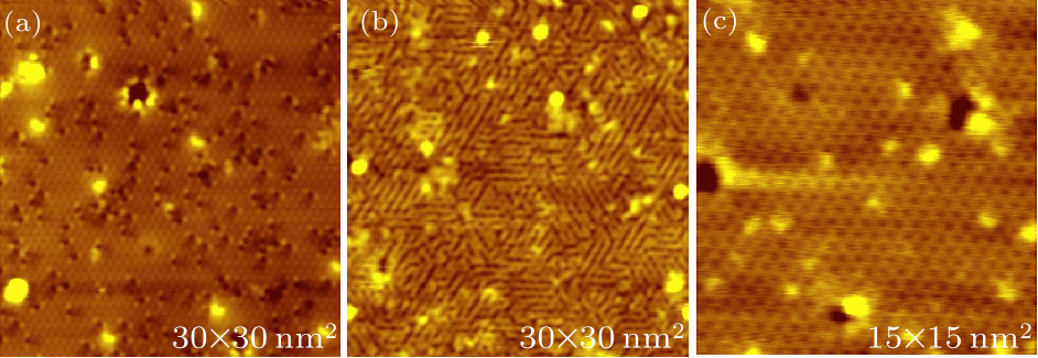
Fig. 2. STM images of (a) a clean monolayer Sn$_{2}$Bi after a small hydrogen exposure, (b) after a large hydrogen exposure and (c) after dehydrogenation. The scanning parameters of (a)–(c) are the same: tip bias $-2$ V and tunneling current 100 pA.
A close-up STM image of the individual hydrogen adsorption sites on the Sn$_{2}$Bi surface is shown in Fig. 3(a). Individual H adsorption sites exhibit as darker spot approximately on the dark centers of the original honeycomb lattice. Another significant feature is that each dark spot is accompanied by a pair of bright wings, and they jointly appear as a butterfly in the high-resolution STM images. Interestingly, the butterfly can have three orientations relevant to the three crystallographic orientations of the Si(111) substrate. The observation of butterfly-like adsorption sites provides rich structural information. Indeed, from the symmetry analysis one can unambiguously determine the adsorption geometry of the H atom in the double-honeycomb lattice of Sn$_{2}$Bi. As we discussed previously, there are three possible adsorption sites: on-top, bridge and hollow. Because individual H adsorption sites exhibit as darker spots approximately on the dark centers of the original honeycomb lattice, where a Sn atom in the second layer is present according to the structure model. At first glance it seems that the H atom is adsorbed on top of the central Sn atom (the T sites). However, this possibility can be excluded by the observation of the accompanying wings. Such a symmetry-breaking feature contradicts with an on-top adsorption model since in that case the three-fold symmetry of the surface should be preserved. On the other hand, the symmetry breaking is consistent with either the bridge site adsorption or the hollow site adsorption pictures. In the hollow site adsorption picture, the hydrogen atom can choose to locate inside one of the three smallest honeycombs around the central Sn atom. However, in this case the mirror symmetric axis should be aligned with the direction which is 30$^{\circ}$ rotated with respected to the experimentally observed mirror symmetric axis of the butterfly. Finally, we can unambiguously derive the bridge site adsorption picture, in which the hydrogen atom is located between the central Sn atom and one of its adjacent Sn atoms. In this picture there are three possible Sn–Sn bridge sites surrounding the central Sn atom, and the mirror symmetric axis of the bridge-adsorption geometry is aligned perfectly in agreement with the orientation of our experimental observation.
cpl-37-6-066802-fig3.png
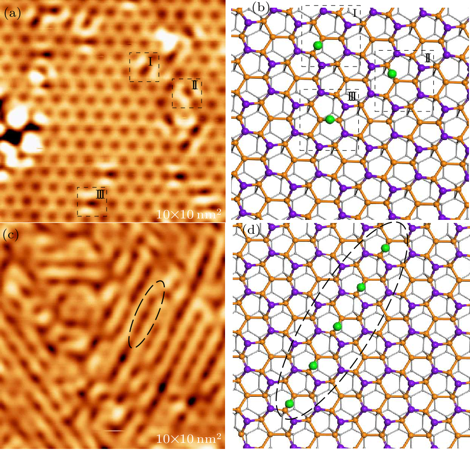
Fig. 3. STM image and structural model of the Sn$_{2}$Bi after hydrogenation with a small and fully hydrogen exposure. (a) A high-resolution STM topography image of Sn$_{2}$Bi with a small hydrogen exposure (tip bias $-2$ V, tunneling current 100 pA). (b) Structural model of (a). The green balls represent hydrogen atoms. (c) A high-resolution STM image of the Sn$_{2}$Bi after fully hydrogenated (tip bias $-2$ V, tunneling current 100 pA). (d) Gully structure models formed by the adsorption of hydrogen atoms in one of the three directions.
In order to further understand the adsorption mechanism, we have carried out first principles calculations. One hydrogen atom is put on top of the central Sn atom. When the structure is fully relaxed, the hydrogen atom spontaneously moves to the bridge site. The adsorption energy of the H atom at the bridge sites has the lowest energy, which further supports the bridge-site adsorption picture. As the hydrogen dose increases, the randomly distributed H adsorption sites interconnect and form dark trenches. A typical fully hydrogenated Sn$_{2}$Bi surface is illustrated in Fig. 3(c). As can be seen from the image, the trenches also have three different directions corresponding to the three-fold symmetry of the substrate. From the structural model of the single hydrogen adsorption site, one can naturally derive the structure model of the trench, as shown in Fig. 3(d). The hydrogen atoms adsorb on continuous Sn–Sn bridge sites forming a two-fold period in this direction. The "wings" of a single H adsorption site are connected along the same direction and form the smooth shoulders of the trench. The formation of the linear two-fold structure on the hydrogen-saturated surface indicates that there are interactions between adjacent H atoms, although they seem to be separated quite far apart. Possible interactions may come from the lattice distortion due to the insertion of hydrogen atoms, and the linear alignment of H atoms could help to relax the induced strain.
cpl-37-6-066802-fig4.png
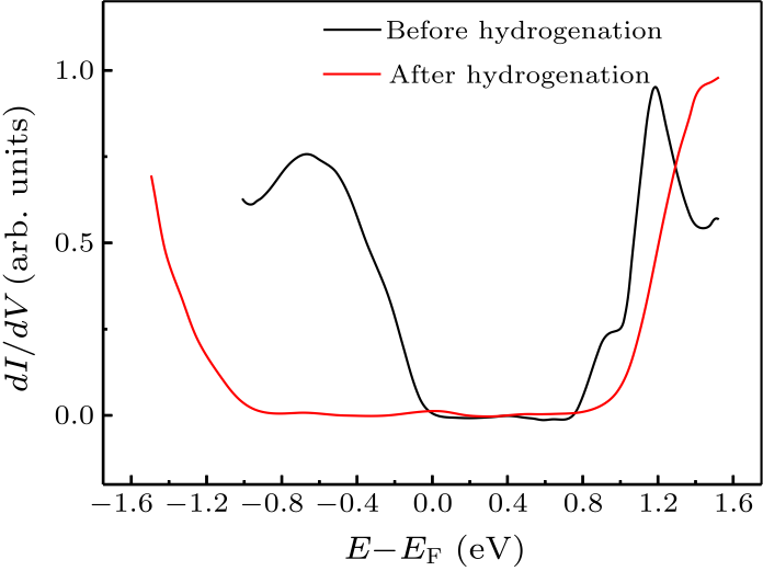
Fig. 4. STS results of Sn$_{2}$Bi before (black curve) and after (red curve) hydrogenation.
The hydrogenation should largely influence the electronic structures of Sn$_{2}$Bi. We have performed scanning tunneling spectroscopy (STS) measurements on hydrogenated 2D Sn$_{2}$Bi. The STS results of 2D Sn$_{2}$Bi before and after hydrogenation are shown in Fig. 4. We find that the hydrogenated sample has a much larger gap than the clean Sn$_{2}$Bi, which is consistent with the computational work.[20] Moreover, in pristine Sn$_{2}$Bi, there is a pronounced peak at 1.1 eV above the Fermi surface which corresponds to the flat band at the bottom of the conduction band of Sn$_{2}$Bi,[18] as clearly revealed in the STS before hydrogenation. This band comes from the central Sn atom in the honeycomb structure. This central isolated Sn atom is distinguished from other Sn atoms that bond with bismuth atoms, resulting in the flat electronic structures at the bottom of the conduction band.[18] Interestingly, after hydrogenation, the flat band totally disappeared in the STS curve (Fig. 4). From our structural model we can see that the hydrogen atoms bond with the central tin atoms and break the structural symmetry, which nicely explains the disappearance of the flat band. This phenomenon also provides additional support to our structural models. Finally, we exploited the dehydrogenation process. In order to verify whether the hydrogenation process is reversible, we heated the hydrogen-saturated sample. When the sample is heated to about 500 K, the trench structure disappears, and the sample comes back to its original state (some big bright protrusions in the image are due to contaminations during H adsorption). As shown in Fig. 2(c), a regular Sn$_{2}$Bi $2 \times 2$ honeycomb lattice is completely restored after hydrogen desorption. Furthermore, we also measured the STS of the sample after hydrogen desorption and the spectra are nearly identical to the clean Sn$_{2}$Bi surface, which further proves that the hydrogenation process is completely reversible. The adsorption-desorption cycle can be repeated many times with the vacuum chamber and the hydrogen gas clean enough. The reversible hydrogenation process may be useful for controllable hydrogen storage. In summary, the hydrogenation of monolayer Sn$_{2}$Bi has been systematically studied by STM and STS. Our STM measurement and DFT calculations reveal that the hydrogen atoms are adsorbed in the bridge sites between the center Sn atom and one of its adjacent Sn atoms. The bridge-site adsorption can be derived by symmetry analysis of the butterfly-like feature of single H adsorption site. At the saturation coverage, there are one-dimensional, trench-like structures in three symmetry directions, indicating certain interaction between neighboring H atoms. Furthermore, the hydrogenation increases the energy gap and vanishes the flat band of monolayer Sn$_{2}$Bi. By heating the fully hydrogenated Sn$_{2}$Bi to about 500 K, dehydrogenation occurs and the surface morphology and electronic properties of the sample was restored to its original state. Our results not only provide experimental support to the double-honeycomb lattice structure of 2D Sn$_{2}$Bi, but also demonstrate the interesting role of hydrogenation in the surface structural determination as well as the modification of surface electronic structures. The hydrogenated Sn$_{2}$Bi exhibits a large band gap, which may be potentially applicable in silicon-based optoelectronics.
References Interaction of hydrogen with solid surfacesStudy by scanning tunneling microscopy of hydrogen adsorption and desorption on Si(111)7×7 at room temperature and at high temperatureAtomic-scale studies of hydrogenated semiconductor surfacesAtomic Hydrogen Adsorbate Structures on GrapheneOrdered and Reversible Hydrogenation of SiliceneFrom Silicene to Half-Silicane by HydrogenationThe importance of structure and bonding in semiconductor surface chemistry: hydrogen on the Si(111)-7 × 7 surfaceBandgap opening in graphene induced by patterned hydrogen adsorptionGraphane: A two-dimensional hydrocarbonAtomic-scale visualization and surface electronic structure of the hydrogenated diamond C ( 100 ) ( 2 × 1 ) : H surfaceTopological Insulating Phases in Two-Dimensional Bismuth-Containing Single Layers Preserved by HydrogenationScanning tunneling microscopy study on initial stage of atomic hydrogen adsorption on the Si(111) 7×7 surfaceElectric Field Effect in Atomically Thin Carbon FilmsEvidence of Silicene in Honeycomb Structures of Silicon on Ag(111)Epitaxial growth of two-dimensional staneneStrain-induced band engineering in monolayer stanene on Sb(111)Epitaxial growth of ultraflat stanene with topological band inversionBinary Two-Dimensional Honeycomb Lattice with Strong Spin-Orbit Coupling and Electron-Hole AsymmetryStabilizing the isolated Sn 2 Bi nanosheet and tailoring its electronic structure by chemical functionalization: A computational studyTuning electronic and optical properties of free-standing Sn 2 Bi monolayer stabilized by hydrogenationThe ultralow thermal conductivity and ultrahigh thermoelectric performance of fluorinated Sn2Bi sheet in room temperatureScanning tunneling microscopy investigations of unoccupied surface states in two-dimensional semiconducting β-√3 × √3-Bi/Si(111) surface
[1] Christmann K 1988 Surf. Sci. Rep. 9 1
[2] Kraus A, Hanbucken M, Neddermeyer H 2002 Anal. Bioanal. Chem. 374 688
[3] Mayne A J, Riedel D, Dujardin G 2006 Prog. Surf. Sci. 81 1
[4] Balog R, Jorgensen B, Wells J, Laegsgaard E, Hofmann P, Hornekaer L 2009 J. Am. Chem. Soc. 131 8744
[5] Qiu J, Fu H, Xu Y, Oreshkin A I, Shao T, Li H, Meng S, Wu K 2015 Phys. Rev. Lett. 114 126101
[6] Qiu J L, Fu H X, Xu Y, Zhou Q, Meng S, Li H, Wu K H 2015 ACS Nano 9 11192
[7] Boland J J 1991 Surf. Sci. 244 1
[8] Balog R, Jorgensen B, Nilsson L, Andersen M, Rienks E, Bianchi M, Fanetti M, Laegsgaard E, Baraldi A, Lizzit S, Sljivancanin Z, Besenbacher F, Hammer B, Pedersen T G, Hornekaer L 2010 Nat. Mater. 9 315
[9] Sofo J O, Barber G D 2007 Phys. Rev. B 75 153401
[10] Bobrov K, Mayne A, Comtet G, Hellner L 2003 Phys. Rev. B 68 195416
[11] Freitas R R Q, Rivelino R, de Brito Mota F, de Castilho C M C, Gueorguiev G K 2015 J. Phys. Chem. C 119 23599
[12] Fukuda T, Nakayama H 2006 Surf. Sci. 600 2443
[13] Novoselov K S, Geim A K, Morozov S V, Jiang D, Zhang Y, Dubonos S V, Firsov A A 2004 Science 306 666
[14] Feng B J, Ding Z J, Meng S, Yao Y G, He X Y, Cheng P, Wu K H 2012 Nano Lett. 12 3507
[15] Zhu F F, Chen W J, Xu Y, Gao C L, Guan D D, Liu C H, Qian D, Jia J F 2015 Nat. Mater. 14 1020
[16] Gou J, Kong L, Li H, Zhong Q, Li W, Cheng P, Chen L and Wu K 2017 Phys. Rev. Mater. 1 054004
[17] Deng J, Xia B, Ma X, Chen H, Shan H, Zhai X, Li B, Xu Y and Duan W 2018 Nat. Mater. 17 1081
[18] Gou J, Xia B, Li H, Wang X, Kong L, Cheng P, Li H, Zhang W, Qian T, Ding H, Xu Y, Duan W, Chen L 2018 Phys. Rev. Lett. 121 126801
[19] Ding Y and Wang Y 2019 Appl. Phys. Lett. 114 073103
[20] Vishkayi S I and Tagani M B 2020 J. Appl. Phys. 127 014302
[21] Li T, Yu J, Zhang B and Sun Q 2020 Nano Energy 67 104283
[22] Gou J, Kong L J, Li W B, Sheng S X, Li H, Meng S, Cheng P, Chen L 2018 Phys. Chem. Chem. Phys. 20 20188